Semiconductor device and manufacturing method thereof, and electronic device

An electronic device and semiconductor technology, which is applied in semiconductor devices, semiconductor/solid-state device manufacturing, circuits, etc., can solve the problems of increasing fin loss and fin consumption, and achieve the effects of easy implementation, avoiding consumption and loss, and simple process

Inactive Publication Date: 2016-08-03
SEMICON MFG INT (SHANGHAI) CORP
View PDF4 Cites 1 Cited by
  • Summary
  • Abstract
  • Description
  • Claims
  • Application Information

AI Technical Summary

Problems solved by technology

However, since oxygen is selected as the process atmosphere and needs to be carried out at high temperature, conventional thermal gate oxide or high-temperature oxidation (high-t

Method used


Image

  • Semiconductor device and manufacturing method thereof, and electronic device
  • Semiconductor device and manufacturing method thereof, and electronic device
  • Semiconductor device and manufacturing method thereof, and electronic device

Examples


Embodiment 1

[0039] In order to solve the problems in the prior art, the present invention provides a method for preparing a semiconductor device. The method will be further described below in conjunction with the accompanying drawings, wherein Figure 2a-2e It is a schematic diagram of the manufacturing process of the semiconductor device in the embodiment of the present invention.

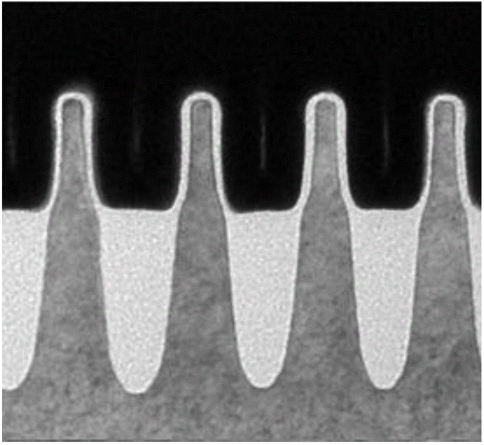
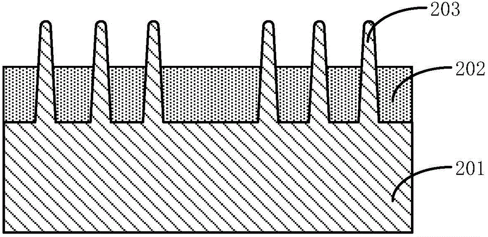
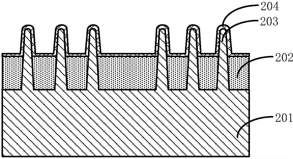
[0040] First, step 201 is performed to provide a semiconductor substrate 201 in which several fins 203 are formed.

[0041] Specifically, such as Figure 2a As shown, the semiconductor substrate may be at least one of the materials mentioned below: silicon, silicon-on-insulator (SOI), silicon-on-insulator (SSOI), silicon-germanium-on-insulator (S-SiGeOI) , silicon germanium on insulator (SiGeOI) and germanium on insulator (GeOI), etc.

[0042] Then pattern the semiconductor substrate to form the fins 203 in the semiconductor substrate. The specific method may include: forming a patterned mask layer, such as...

Embodiment 2

[0074] The present invention also provides a semiconductor device, which is prepared by the method described in Embodiment 1. The fin pattern in the semiconductor device prepared by the method of the invention is not lost due to oxidation, and the pattern has good uniformity and consistency, so as to further improve the performance and yield of the semiconductor device.

Embodiment 3

[0076] The present invention also provides an electronic device, including the semiconductor device described in Embodiment 2. Wherein, the semiconductor device is the semiconductor device described in Embodiment 2, or the semiconductor device obtained according to the preparation method described in Embodiment 1.

[0077] The electronic device of this embodiment can be any electronic product or equipment such as mobile phone, tablet computer, notebook computer, netbook, game console, TV set, VCD, DVD, navigator, camera, video recorder, voice recorder, MP3, MP4, PSP, etc. , can also be any intermediate product including the semiconductor device. The electronic device according to the embodiment of the present invention has better performance due to the use of the above-mentioned semiconductor device.


PUM


Abstract

The invention relates to a semiconductor device and a manufacturing method thereof, and an electronic device. The method comprises steps: S1, a semiconductor substrate is provided, and a plurality of mutually-spaced fins are formed on the semiconductor substrate; S2, a sacrificial layer is formed on the surface of each fin to cover the fin; S3, a method generated by in-situ steam is selected to form an oxide layer on the surface of the sacrificial layer, an in-situ steam generation oxidation process is executed at the same time, the sacrificial layer is converted into an oxide, and a gate oxide is formed on the surface of the fin. The method of the invention has the advantages that an atomic layer deposition or molecular layer deposition method is selected to form the sacrificial layer, and consumption and loss of the fins are reduced; good conformal property is provided by selecting the atomic layer deposition or molecular layer deposition method; and ISSG oxidation happens on the thin sacrificial layer SiN, the SiN is finally converted into SiO2, and oxidation of the fins does not happen.

Description

technical field [0001] The present invention relates to the field of semiconductors, in particular, the present invention relates to a semiconductor device, a preparation method thereof, and an electronic device. Background technique [0002] With the continuous development of semiconductor technology, in order to improve the performance of the device, the size of integrated circuit devices needs to be continuously reduced. With the continuous reduction of the size of CMOS devices, the development of three-dimensional designs such as fin field effect transistors (FinFET) has been promoted. [0003] Compared with the existing planar transistors, the FinFET device has more superior performance in terms of channel control and reducing shallow channel effects; the planar gate structure is arranged above the channel, and the gate in the FinFET The fins are arranged around the fins, so static electricity can be controlled from three sides, and the performance in static electricity...

Claims


Application Information

Patent Timeline
IPC IPC(8): H01L29/423H01L29/78H01L21/28H01L21/336
Inventor 赵海陈正领
Owner SEMICON MFG INT (SHANGHAI) CORP
Why Eureka
Try Eureka