A kind of preparation method of fpc board with low loss and high flexibility of high frequency transmission
A high-frequency transmission, high-flexibility technology, applied in printed circuit manufacturing, lamination of printed circuit boards, reduction of crosstalk/noise/electromagnetic interference (etc.) Reduce and other problems to achieve the effect of improving flexibility, achieving high integration, and reducing the thickness of copper layers
- Summary
- Abstract
- Description
- Claims
- Application Information
AI Technical Summary
Problems solved by technology
Method used
Image
Examples
Embodiment 1
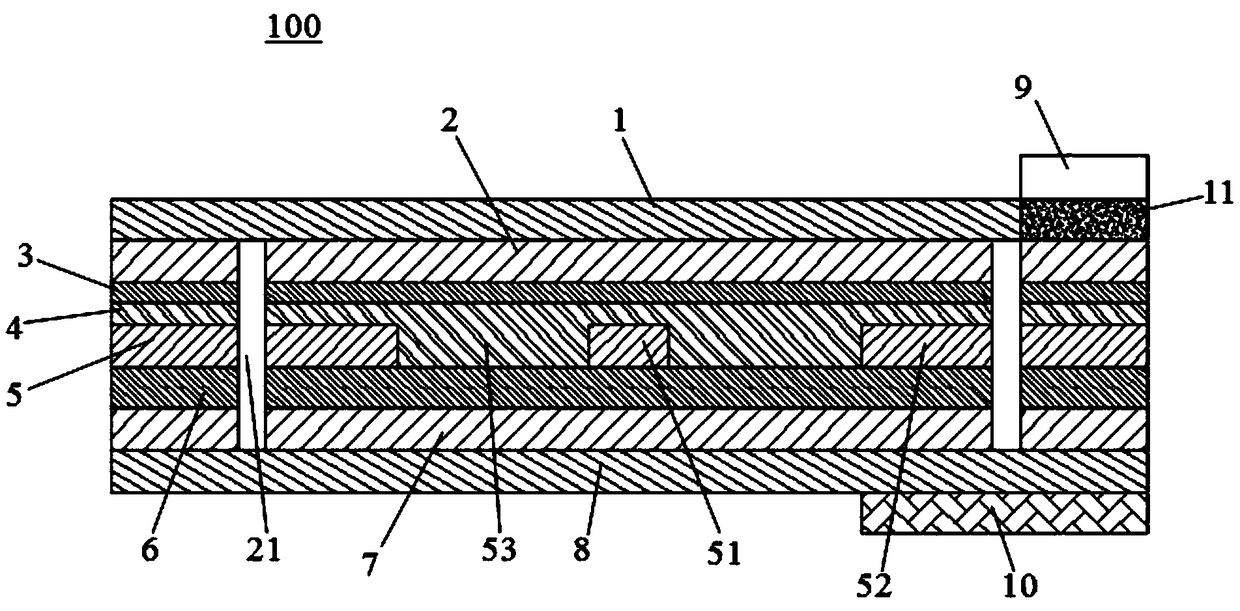
[0035] Please refer to figure 1 In this embodiment, a low-loss, high-flexibility, and high-frequency transmission FPC board 100 has a cross-sectional structure sequentially including a first solder resist layer 1, a first shielding layer 2, a first dielectric layer 3, and an adhesive layer from top to bottom. 4. Transmission line layer 5 , second dielectric layer 6 , second shielding layer 7 , and second solder resist layer 8 .
[0036] The transmission line layer 5 includes a signal line 51 formed on a central axis, and transmission areas 52 symmetrically distributed along the signal line 51 . A distance 53 is provided between the signal line 51 and the transmission area 52 .
[0037] The first solder resist layer 1 and the second solder resist layer 8 are flexible bending-resistant inks with a thickness of 12um, which are mainly used to prevent the surface of the first shield layer 2 and the second shield layer 7 made of metal from being oxidized. The surface of the first ...
Embodiment 2
[0075] The content of the second embodiment is basically the same as that of the first embodiment, the difference is that: the thickness of the first solder resist layer 1 and the second solder resist layer 8 is 18um; the thickness of the first shielding layer 2 and the second shielding layer 7 The thickness of the first dielectric layer 3 is 30um; the thickness of the bonding layer 4 is 18um; the thickness of the transmission line layer 5 is 20um; the thickness of the second dielectric layer 6 is 48um; the thickness of the reinforcing layer 10 is 1300um; The hole 21 is directly 0.15mm.
Embodiment 3
[0077] The content of the third embodiment is basically the same as that of the first embodiment, the difference is that: the thickness of the first solder resist layer 1 and the second solder resist layer 8 is 25um; the thickness of the first shielding layer 2 and the second shielding layer 7 The thickness of the first dielectric layer 3 is 50um; the thickness of the bonding layer 4 is 25um; the thickness of the transmission line layer 5 is 28um; the thickness of the second dielectric layer 6 is 75um; the thickness of the reinforcing layer 10 is 2500um; The hole 21 is directly 0.2mm.
PUM
 Abstract
Description
Claims
Application Information
