Difference etching solution for semi-additive process preparation fine line

A technology of differential etching and fine lines, applied in chemical/electrolytic methods to remove conductive materials, etc., can solve problems such as difficulty in controlling high-frequency line impedance, insufficient selectivity of copper-reducing solution, and inability to maintain rectangular shape, achieving macroscopic The vision is clean and bright, the side etching effect is improved, and the effect of impedance control is beneficial.

Inactive Publication Date: 2016-08-10
杭州乐芙新材料科技有限公司
View PDF2 Cites 9 Cited by
  • Summary
  • Abstract
  • Description
  • Claims
  • Application Information

AI Technical Summary

Problems solved by technology

[0003] However, the conventional differential etching solution uses a copper-reducing solution, which has a strong side erosion effect on the copper surface after pattern electroplating, and the solution is more likely to attack the side wall of the circuit, and because the selectivity of the copper-reducing solution is not strong enough, in real In the current SAP process, it is difficult to etch only the bottom copper, while having good protection for the circuit or a relatively slow etching effect
Therefore, the use of copper-reducing solution for differential etching process can easily lead to floating of a large number of lines, which is called Undercut in the industry, and it is difficult to improve the yield rate, especially for the preparation of fine lines with line width / line spacing below 20μm / 20μm. Ordinary copper-reducing solution The yield rate of this kind of fine lines is extremely low
In addition, during differential etching, the edges and corners of the line are bitten by the etching solution in two directions. If there is no protection mechanism, the rectangular shape of the line cross-section will not be maintained, making it difficult to control the impedance of high-frequency lines.

Method used


Image

  • Difference etching solution for semi-additive process preparation fine line
  • Difference etching solution for semi-additive process preparation fine line
  • Difference etching solution for semi-additive process preparation fine line

Examples


Embodiment 1

[0021] Prepare a differential etching solution according to the following ratio, where the solvent is deionized water, and prepare 800L of solution.

[0022]

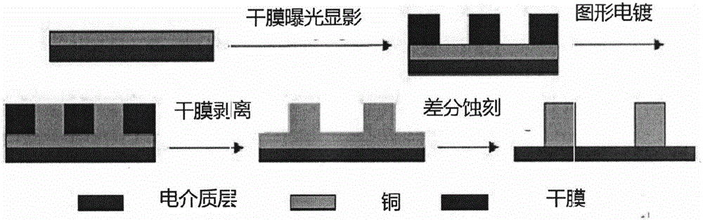
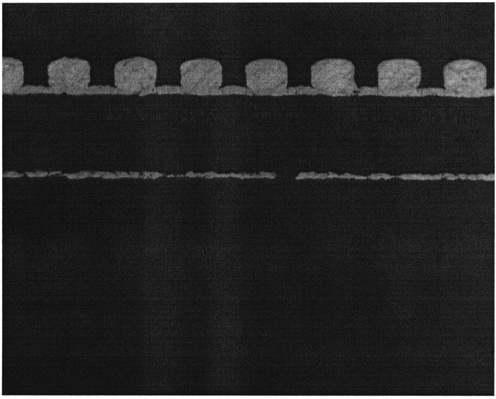
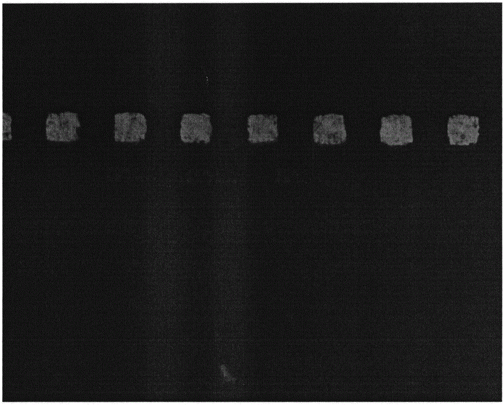
[0023] Put the prepared solution into the horizontal differential etching production equipment, set the corresponding speed according to the length of the treatment tank, check the differential etching rate, observe the line section through a metallographic microscope after differential etching, and observe whether there is side etching and bottom etching. Whether the copper is removed cleanly, whether the cross-section of the circuit remains a good rectangle, and at the same time observe the microscopic morphology of the circuit surface through the scanning electron microscope, and whether it has a certain roughness. The metallographic section pictures of the line section before and after differential etching are as follows: figure 2 and image 3 as shown, Figure 4 It is the SEM picture of the circuit topography...


PUM

PropertyMeasurementUnit
surface roughnessaaaaaaaaaa

Abstract

The present invention provides a difference etching solution for a semi-additive process preparation fine line. The difference etching solution comprises two parts: basic solution and difference etching additive, wherein the basic solution is vitriol and hydrogen peroxide, and the difference etching additive includes a hydrogen peroxide stabilizer, a flat etchant protective agent, a gloss agent and a roughness control agent. Compared with the prior art, the difference etching solution for semi-additive process preparation fine line is able to effectively remove the base copper and effectively reduce the lateral erosion. The difference etching solution for a semi-additive process preparation fine line employs a lateral erosion protective agent so as to greatly reduce the generation of Undercut, improve the line yield rate, effectively protect the line corner angle and maintain the rectangular morphology of the line cross section; and the difference etching solution for the semi-additive process preparation fine line employs additives such as a microetching detergent, a roughness control agent and the like so as to perform further control of the line microscopic morphology of the line after difference etching, obtain visual sense shine and cleaning and facilitate subsequent process connection because of the roughness of 0.2-0.5[Mu]m in the microscopic scale.

Description

technical field [0001] The invention relates to a differential etching solution used in the preparation of high-precision circuits by a semi-additive (Semi-additive process, SAP) process. Background technique [0002] Etching is an important process for preparing circuits in the field of printed circuit boards and semiconductors. It is difficult to prepare fine circuits with a line width / space below 20μm / 20μm by ordinary etching processes. Usually, such circuits can only be prepared by semi-additive methods. The specific process is as figure 1 shown. [0003] However, the conventional differential etching solution uses a copper-reducing solution, which has a strong side erosion effect on the copper surface after pattern electroplating, and the solution is more likely to attack the side wall of the circuit, and because the selectivity of the copper-reducing solution is not strong enough, in real In the current SAP process, it is difficult to only etch the bottom copper, but...

Claims


Application Information

Patent Timeline
Patent Type & Authority Applications(China)
IPC IPC(8): H05K3/06C23F1/18
Inventor 王靖张斌过勇
Owner 杭州乐芙新材料科技有限公司
Why Eureka
Try Eureka