Semiconductor device and forming method of semiconductor device

A semiconductor and device technology, applied in the field of semiconductor devices and their formation, can solve the problems of increased drain current, decreased gate threshold voltage, increased number of electrons, etc. Effect

Inactive Publication Date: 2016-08-17
INST OF MICROELECTRONICS CHINESE ACAD OF SCI
View PDF5 Cites 6 Cited by
  • Summary
  • Abstract
  • Description
  • Claims
  • Application Information

AI Technical Summary

Problems solved by technology

[0002] With the high integration of semiconductor devices, the channel length of the device continues to shrink, and the short channel effect becomes more and more significant. The short channel effect will deteriorate the electrical performance of the device, such as causing a decrease in the gate threshold voltage, an increase in power consumption, and a decrease in signal-to-noise ratio. and other issues become the dominant factors affecting device performance
[0003] The DIBL (Drain Induced Barrier Lowering) effect, that is, the barrier lowering effect introduced by the drain, is one of the short channel effects. After the channel length decreases and the voltage Vds increases, the depletion layer of the drain and source junctions Closer, the barrier height of the source terminal decreases, so the number of electrons injected into the channel by the source region increases, and the drain current increases, which reduces the threshold voltage of the device and affects the overall performance of the device. Moreover, as the size of the device continues to decrease, The DIBL effect is more severe

Method used


Image

  • Semiconductor device and forming method of semiconductor device
  • Semiconductor device and forming method of semiconductor device
  • Semiconductor device and forming method of semiconductor device

Examples


Embodiment Construction

[0027] Embodiments of the present invention are described in detail below, examples of which are shown in the drawings, wherein the same or similar reference numerals designate the same or similar elements or elements having the same or similar functions throughout. The embodiments described below by referring to the figures are exemplary only for explaining the present invention and should not be construed as limiting the present invention.

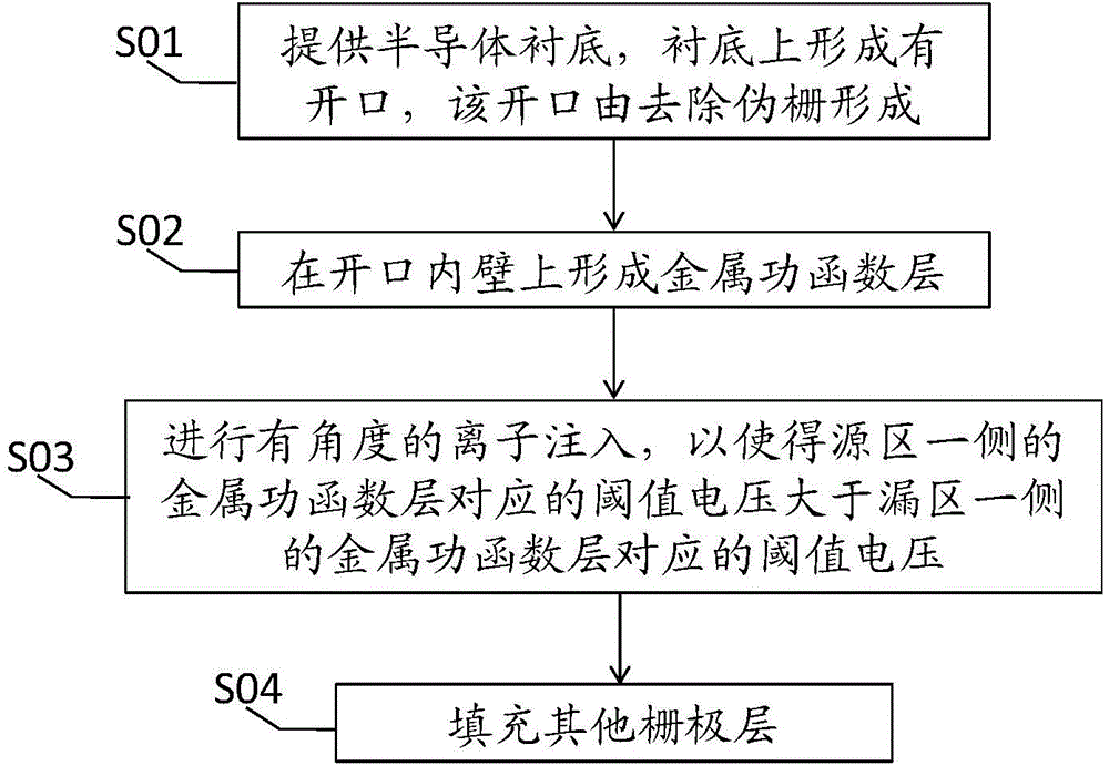
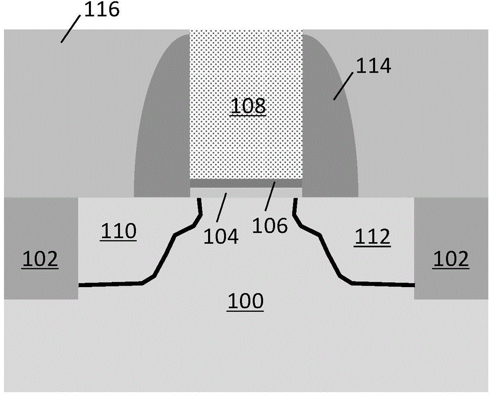
[0028] The present invention proposes a method for manufacturing a semiconductor device, referring to figure 1 As shown, it includes: providing a semiconductor substrate with an opening formed on the substrate, and the opening is formed by removing the dummy gate; forming a metal work function layer on the inner wall of the opening; performing ion implantation at an angle so that the metal on the side of the source region The threshold voltage corresponding to the work function layer is greater than the threshold voltage corresponding to...


PUM


Abstract

The invention provides a manufacturing method of a semiconductor device. The method includes the following steps that: a semiconductor substrate is provided, an opening is formed in the substrate, and the opening is formed by removing a dummy gate; metal work function layers are formed at the internal wall of the opening; ion implantation of a certain angle is carried out, so that threshold voltage corresponding to a metal work function layer at one side of a source region is larger than threshold voltage corresponding to a metal work function layer at one side of a drain region; and other grid layers are filled. According to the manufacturing method of the invention, voltage drop of a channel region near a source end is increased, and voltage drop of a channel region near a drain end is decreased, and therefore, the electric field of the drain end can be decreased, and short-channel effects such as DIBL (drain induced barrier lowering) can be suppressed, and the electric field of the source end is increased, so that the transport speed of carriers can be improved, and the performance of the device can be improved.

Description

technical field [0001] The invention relates to the field of semiconductor devices, in particular to a semiconductor device and a forming method thereof. Background technique [0002] With the high integration of semiconductor devices, the channel length of the device continues to shrink, and the short channel effect becomes more and more significant. The short channel effect will deteriorate the electrical performance of the device, such as causing a decrease in the gate threshold voltage, an increase in power consumption, and a decrease in signal-to-noise ratio. and other issues become the dominant factors affecting device performance. [0003] The DIBL (Drain Induced Barrier Lowering) effect, that is, the barrier lowering effect introduced by the drain, is one of the short channel effects. After the channel length decreases and the voltage Vds increases, the depletion layer of the drain and source junctions Closer, the barrier height of the source terminal decreases, so ...

Claims


Application Information

Patent Timeline
Patent Type & Authority Applications(China)
IPC IPC(8): H01L21/336H01L21/265H01L29/78H01L29/423
Inventor 张严波殷华湘朱慧珑
Owner INST OF MICROELECTRONICS CHINESE ACAD OF SCI
Why Eureka
Try Eureka