
A kind of co-sputtering method prepares the method for absorbing layer of cigs thin film solar cell

A solar cell and co-sputtering technology, which is applied in circuits, photovoltaic power generation, electrical components, etc., can solve the problems of CIGS absorption layer stoichiometric ratio deviation from the original ratio, indium element sputtering efficiency is low, etc., and is conducive to large-scale industrial production , surface uniformity, enhanced completeness and crystallinity

Inactive Publication Date: 2017-04-05
HENAN UNIVERSITY
View PDF3 Cites 0 Cited by
  • Summary
  • Abstract
  • Description
  • Claims
  • Application Information

AI Technical Summary

Problems solved by technology

[0003] Among the many technologies for preparing CIGS absorbing layer, the preparation of CIGS thin-film solar cells by magnetron sputtering is easy to achieve large-scale production. The most convenient preparation method is to directly sputter CIGS quaternary targets. The sputtering rates of different elements are not the same, especially the sputtering efficiency of indium element is low, which will cause a large deviation between the stoichiometric ratio of the prepared CIGS absorber layer and the original ratio of the target.

Method used


Image

  • A kind of co-sputtering method prepares the method for absorbing layer of cigs thin film solar cell
  • A kind of co-sputtering method prepares the method for absorbing layer of cigs thin film solar cell
  • A kind of co-sputtering method prepares the method for absorbing layer of cigs thin film solar cell

Examples


Embodiment 1

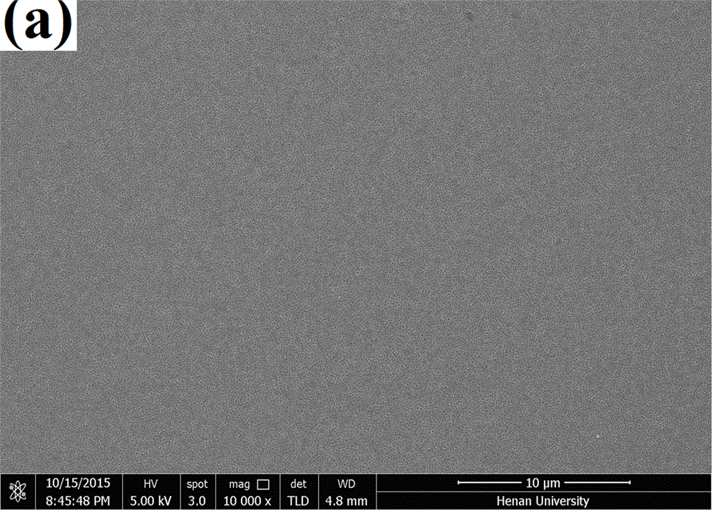
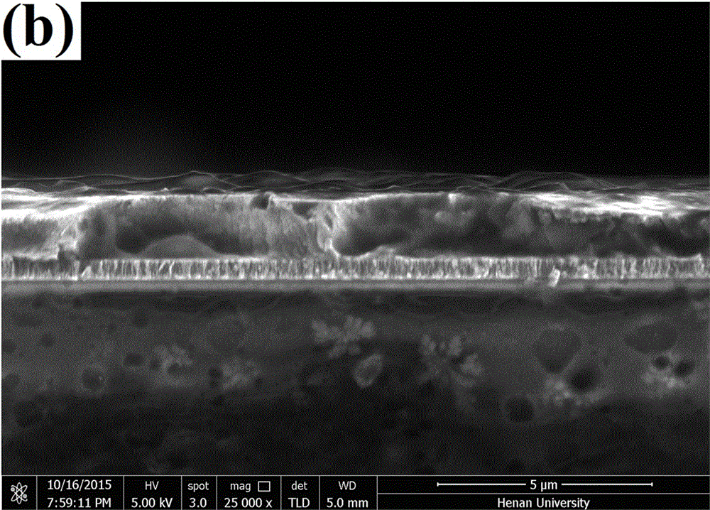
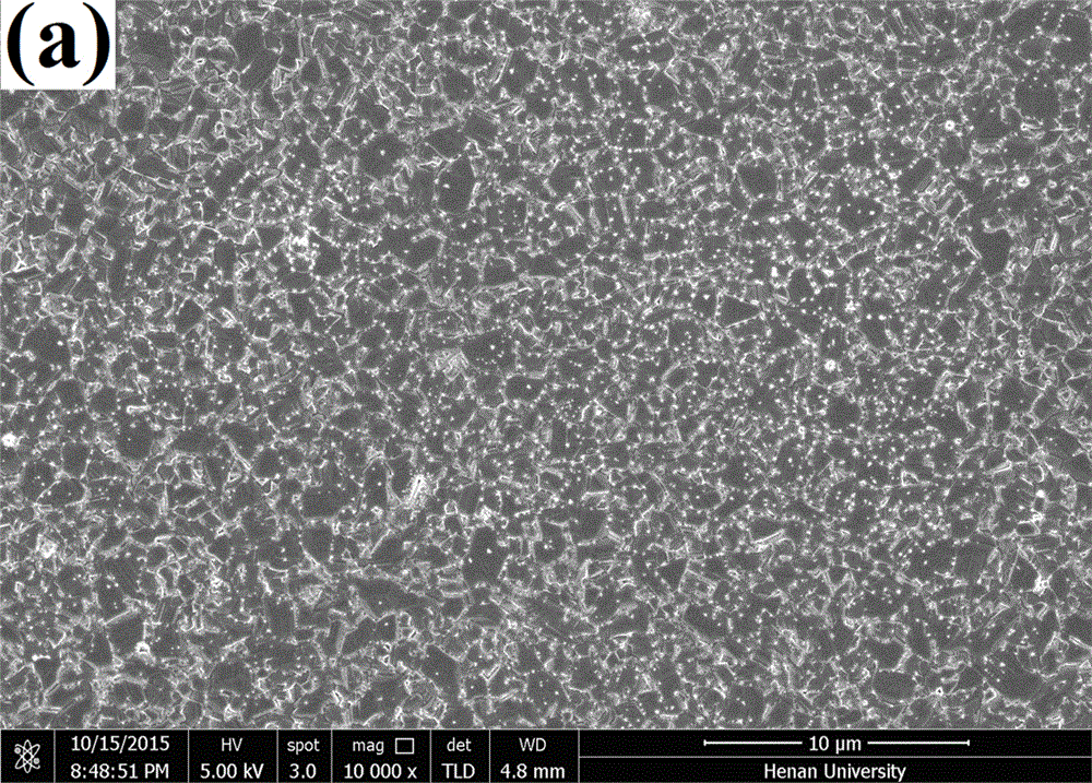
[0016] A kind of co-sputtering method prepares the method for absorbing layer of CIGS thin-film solar cell, comprises the following steps: 1. provides the soda lime glass substrate of molybdenum plating, adopts copper indium gallium selenide target to carry out radio frequency sputtering, adopts indium target to carry out DC sputtering at the same time, The copper indium gallium selenide prefabricated layer was prepared by co-sputtering; the process conditions of co-sputtering are: the vacuum degree of the bulk reaches 8×10 -4 Below Pa, during the sputtering process, the target distance is maintained at 8 cm, the argon gas flow rate is 20 sccm, the substrate rotation speed is 20 r / min, the working pressure is 0.5 Pa, and the co-sputtering time is 120 min. The copper indium gallium selenide target The RF sputtering power of the indium target is 110 W, and the power of the indium target DC sputtering is 70 W; ②Put the prefabricated copper indium gallium selenium layer into a rapi...

Embodiment 2

[0021] A kind of co-sputtering method prepares the method for absorbing layer of CIGS thin-film solar cell, comprises the following steps: 1. provides the soda lime glass substrate of molybdenum plating, adopts copper indium gallium selenide target to carry out radio frequency sputtering, adopts indium target to carry out DC sputtering at the same time, The copper indium gallium selenide prefabricated layer was prepared by co-sputtering; the process conditions of co-sputtering are: the vacuum degree of the bulk reaches 7×10 -4 Below Pa, during the sputtering process, the target distance is maintained at 8 cm, the argon gas flow rate is 20 sccm, the substrate rotation speed is 20 r / min, the working pressure is 0.5 Pa, and the co-sputtering time is 120 min. The copper indium gallium selenide target The RF sputtering power of the indium target is 110 W, and the power of the indium target DC sputtering is 70 W; ② Put the prefabricated layer of copper indium gallium selenium into a ...

Embodiment 3

[0024] A kind of co-sputtering method prepares the method for absorbing layer of CIGS thin-film solar cell, comprises the following steps: 1. provides the soda lime glass substrate of molybdenum plating, adopts copper indium gallium selenide target to carry out radio frequency sputtering, adopts indium target to carry out DC sputtering at the same time, The copper indium gallium selenide prefabricated layer was prepared by co-sputtering; the process conditions of co-sputtering are: the vacuum degree of the bulk reaches 8×10 -4 Below Pa, during the sputtering process, the target distance is maintained at 8 cm, the argon gas flow rate is 20 sccm, the substrate rotation speed is 20 r / min, the working pressure is 0.5 Pa, and the co-sputtering time is 120 min. The copper indium gallium selenide target The RF sputtering power of the indium target is 110 W, and the power of the indium target DC sputtering is 70 W; ②Put the prefabricated copper indium gallium selenium layer into a rapi...


PUM


Abstract

The invention belongs to a method for preparing a CIGS thin-film solar cell absorption layer employing a co-sputtering method. The method comprises the steps as follows: (1) a substrate is provided, radio-frequency sputtering is carried out by a copper indium gallium selenide target, meanwhile, DC sputtering is carried out by an indium target and a copper indium gallium selenide preformed layer is prepared in a co-sputtering manner; and (2) the copper indium gallium selenide preformed layer is put into a quick annealing furnace, is selenized under nitrogen protection for twice and is naturally cooled to a room temperature to obtain the CIGS thin-film solar cell absorption layer. By a technological approach of carrying out sputtering by a standard CIGS quaternary target, large-scale industrial production is facilitated; the loss of an indium element caused by the standard CIGS quaternary target in the sputtering process can be effectively avoided through the method; and a CIGS absorption layer material in accordance with the stoichiometric ratio can be obtained. Annealing treatment is carried out on the prepared CIGS absorption layer through a two-step heating method; the selenylation completeness and crystallinity can be further strengthened; and the high-quality CIGS with a uniform surface and a consistent thickness can be obtained.

Description

technical field [0001] The invention belongs to the field of photoelectric functional materials and thin-film photovoltaic devices, and in particular relates to a method for preparing CIGS thin-film solar cell absorption layers by a co-sputtering method. Background technique [0002] In the first decade of the 21st century, with people's deepening awareness of the depletion of traditional fossil energy and increasing awareness of environmental protection, the development of new energy has entered the fast lane. All kinds of new energy science and technology are moving from laboratory research to industrial application, gradually changing people's production and lifestyle. An industrial revolution based on new energy has slowly kicked off. The research on thin-film solar cells has developed rapidly in recent years and has become the most active direction in the field of solar cells. Among them, copper indium gallium selenide is particularly eye-catching. It is the best solar...

Claims


Application Information

Patent Timeline
Patent Type & Authority Patents(China)
IPC IPC(8): H01L31/18
CPCH01L31/0322Y02E10/541Y02P70/50
Inventor 杜祖亮程轲黄玉茜
Owner HENAN UNIVERSITY
Learn More