A quantum dot superluminescent light-emitting diode and its manufacturing method

A technology of superluminescence and fabrication method, applied in the field of quantum dot superluminescence light-emitting diodes and their fabrication, to achieve the effects of widening gain spectrum, reducing feedback, and optimizing output spectrum

Active Publication Date: 2018-02-16
FUJIAN INST OF RES ON THE STRUCTURE OF MATTER CHINESE ACAD OF SCI
View PDF3 Cites 0 Cited by
  • Summary
  • Abstract
  • Description
  • Claims
  • Application Information

AI Technical Summary

Problems solved by technology

At present, there are still some problems in SLD. It is necessary to optimize the material design and structure of SLD, further improve the output power of the device, broaden the spectral width, etc.

Method used


Image

  • A quantum dot superluminescent light-emitting diode and its manufacturing method
  • A quantum dot superluminescent light-emitting diode and its manufacturing method
  • A quantum dot superluminescent light-emitting diode and its manufacturing method

Examples


Embodiment 1

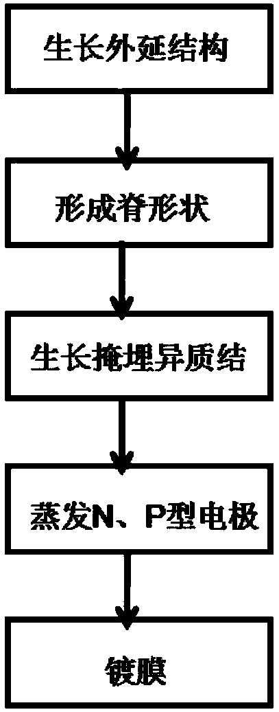
[0033] A kind of fabrication method of quantum dot superluminescent light-emitting diode that the present invention proposes, such as figure 1 As shown, the method includes the following steps:

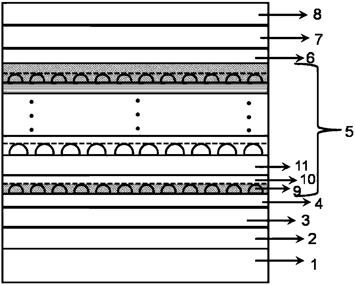
[0034] 1. One epitaxial growth step: such as figure 2 As shown, the epitaxial structure is grown once by MBE, and its structure is sequential along the crystal direction (such as figure 2 shown bottom to top) including N + -GaAs substrate layer 1, N-GaAs buffer layer 2, N-AlGaAs cladding layer 3, AlGaAs lower confinement layer 4, active region 5 containing four layers of InAs quantum dots, AlGaAs upper confinement layer 6, P-AlGaAs cladding layer 7 , P-GaAs protective layer 8 .

[0035] The active region 5 includes a first undoped GaAs layer, four layers of InAs quantum dots and a second undoped GaAs layer, each layer of InAs quantum dots includes InAs quantum dots 9 , an InGaAs capping layer 10 and a GaAs capping layer 11 .

[0036] During the growth of the active region, the l...

Embodiment 2

[0042] This embodiment is a preferred embodiment based on Embodiment 1. The fabrication method of the quantum dot superluminescent light-emitting diode proposed by the present invention is as follows: figure 1 As shown, the method includes:

[0043] 1. One epitaxial growth step: such as figure 2 shown, at N + -GaAs substrate 1, MBE growth doping concentration 1×10 at 500°C 18 200nm N-GaAs buffer layer 2, doping concentration 1×10 18 100nm N-AlGaAs cladding layer 3, 200nm AlGaAs lower confinement layer 4, active region 5 containing four layers of InAs quantum dots, then 200nm AlGaAs upper confinement layer 6 grown at 500°C, doping concentration 1×10 18 100nm P-AlGaAs cladding layer 7, doping concentration 1×10 18 The 10nm P-GaAs protective layer 8 completes an epitaxial growth, and its structure is as follows figure 2 shown.

[0044] The growth method of the active region 5 is as follows: grow a 100nm undoped GaAs layer at 500°C, grow 2ML (ML: atomic layer) InAs qu...

Embodiment 3

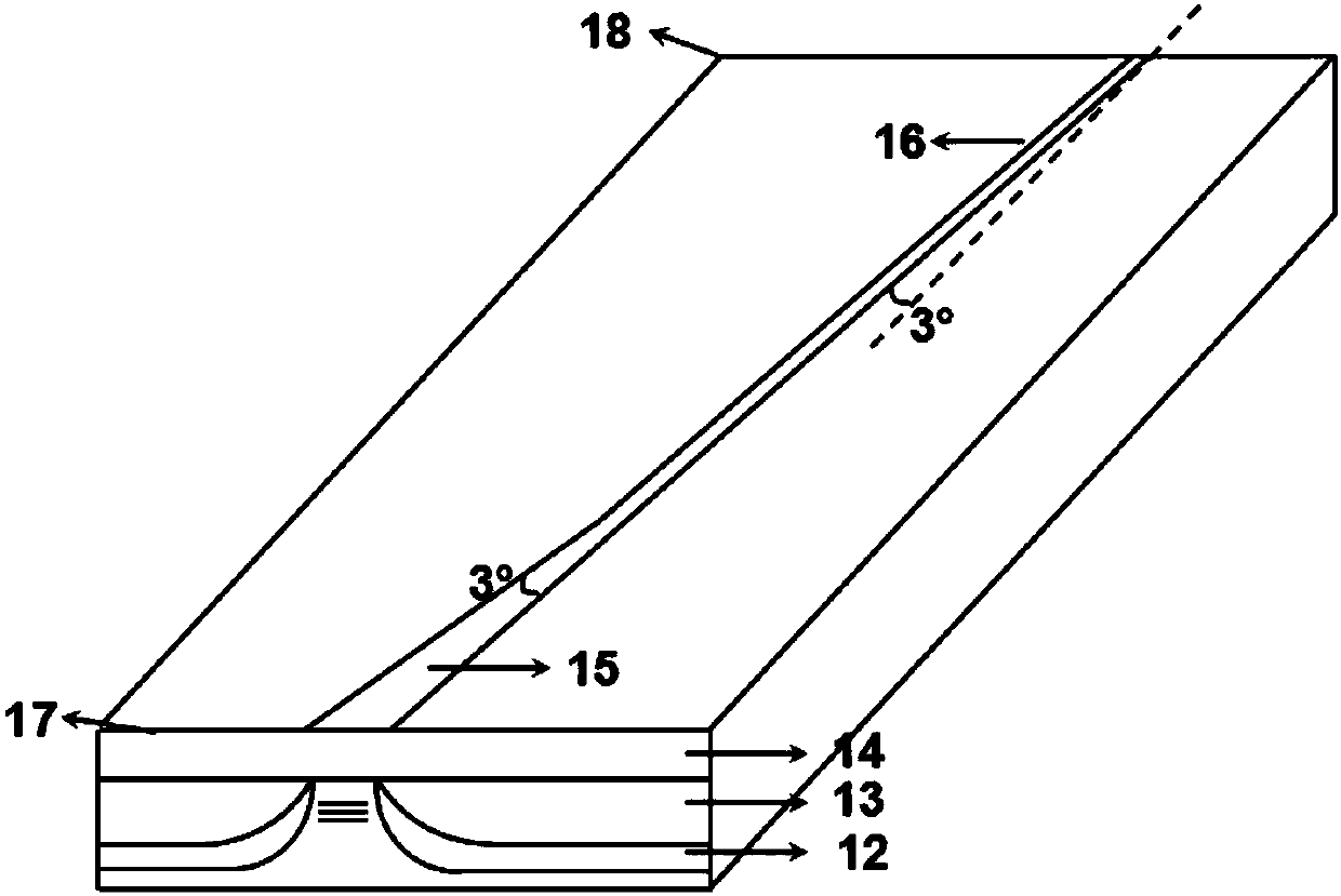
[0050] The quantum dot superluminescent light-emitting diode proposed by the present invention is as figure 2 and image 3 As shown, the quantum dot superluminescent light-emitting diode includes: a primary epitaxial structure and a buried heterojunction structure, wherein the primary epitaxial structure includes: N + -GaAs substrate layer 1, N-GaAs buffer layer 2, N-AlGaAs cladding layer 3, AlGaAs lower confinement layer 4, active region 5 containing four layers of InAs quantum dots, AlGaAs upper confinement layer 6 and P-AlGaAs cladding layer 7 ; Wherein the active region 5 includes a first undoped GaAs layer, four layers of InAs quantum dots and a second undoped GaAs layer arranged in sequence along the crystal direction.

[0051] The N-AlGaAs cladding layer 3, the AlGaAs lower confinement layer 4, the active region 5 containing four layers of InAs quantum dots, the AlGaAs upper confinement layer 6 and the P-AlGaAs cladding layer 7 form a ridge structure along the crystal d...


PUM


Abstract

The invention relates to a manufacturing method of a quantum dot super luminescent diode. The method includes the following steps of primary epitaxial growth, wherein a primary epitaxial structure is grown through MBE and structurally comprises an N+-GaAs substrate layer (1), an N-GaAs buffer layer (2), an N-AlGaAs covering layer (3), an AlGaAs lower limiting layer (4), an active area (5) containing multiple layers of InAs quantum dots, an AlGaAs upper limiting layer (6), a P-AlGaAs covering layer (7) and a P-GaAs protecting layer (8) in sequence in the crystal orientation; formation of a ridge shape; growth of a buried heterojunction; evaporation of an N-type electrode and a P-type electrode; coating. The invention further provides the quantum dot super luminescent diode. The quantum dot super luminescent diode has the advantages of being high in power, capable of achieving wide spectrum output and low in jitter.

Description

technical field [0001] The invention relates to a light-emitting diode, in particular to a quantum dot super-radiant light-emitting diode and a manufacturing method thereof. Background technique [0002] Superluminescent Diodes (SLD) is a highly stable light source with high output power and wide spectral range, which has a wider emission spectrum and lower coherence length than semiconductor lasers; compared with light-emitting diodes, it has Higher output power, widely used in OCT (optical coherence tomography) imaging, fiber optic gyroscope, fiber optic sensor and other systems. For the SLD light source currently used in OCT (optical coherence tomography) with a wavelength of 800nm, the backscattering caused by its narrow spectral width and short peak wavelength greatly affects the imaging resolution and Detection sensitivity. Therefore, how to further increase the peak wavelength of the light source and increase the spectral width is an important method to improve the ...

Claims


Application Information

Patent Timeline
Patent Type & Authority Patents(China)
IPC IPC(8): H01L33/00H01L33/04
CPCH01L33/0045H01L33/0075H01L33/04
Inventor 訾慧薛正群苏辉王凌华林琦林中晞陈阳华
Owner FUJIAN INST OF RES ON THE STRUCTURE OF MATTER CHINESE ACAD OF SCI
Why Eureka
Try Eureka