Light-emitting diode epitaxial wafer and growth method thereof

A technology for light emitting diodes and a growth method, applied in the field of light emitting diode epitaxial wafers and their growth, can solve problems such as reducing the functionality and reliability of LEDs, and achieve the effects of reducing parasitic reactions, improving energy levels, and increasing impedance

Active Publication Date: 2016-08-17
HC SEMITEK SUZHOU
View PDF5 Cites 12 Cited by
  • Summary
  • Abstract
  • Description
  • Claims
  • Application Information

AI Technical Summary

Problems solved by technology

[0005] There is a lattice mismatch between sapphire and GaN, and the defects caused by the lattice mismatch extend to the active layer along the growth direction of the LED, affecting the recombination of electrons and holes in the active layer and causing leakage, reducing the function of the LED sex and reliability

Method used


Image

  • Light-emitting diode epitaxial wafer and growth method thereof
  • Light-emitting diode epitaxial wafer and growth method thereof

Examples


Embodiment 1

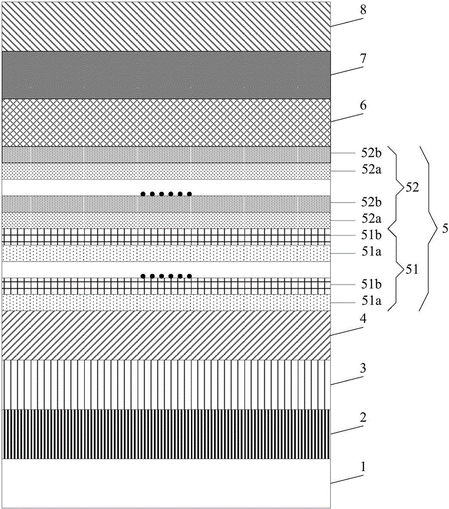
[0032] An embodiment of the present invention provides a light emitting diode epitaxial wafer, see figure 1 , the light-emitting diode epitaxial wafer includes a sapphire substrate 1, and a low-temperature buffer layer 2, a high-temperature buffer layer 3, an N-type layer 4, a defect blocking layer 5, an active layer 6, and an electron blocking layer sequentially stacked on the sapphire substrate 1 7. P-type layer 8.

[0033] In this embodiment, the defect barrier layer 5 includes a first sublayer 51 and a second sublayer 52 stacked on the N-type layer 4 in sequence, and the first sublayer 51 includes alternately stacked first AlGaN layers 51a and GaN layers 51b , the second sub-layer 52 includes alternately stacked second AlGaN layers 52a and third AlGaN layers 52b. The Al content in the first AlGaN layer 51a gradually changes along the growth direction of the light-emitting diode epitaxial wafer, the Al content in the second AlGaN layer 52a and the Al content in the third A...

Embodiment 2

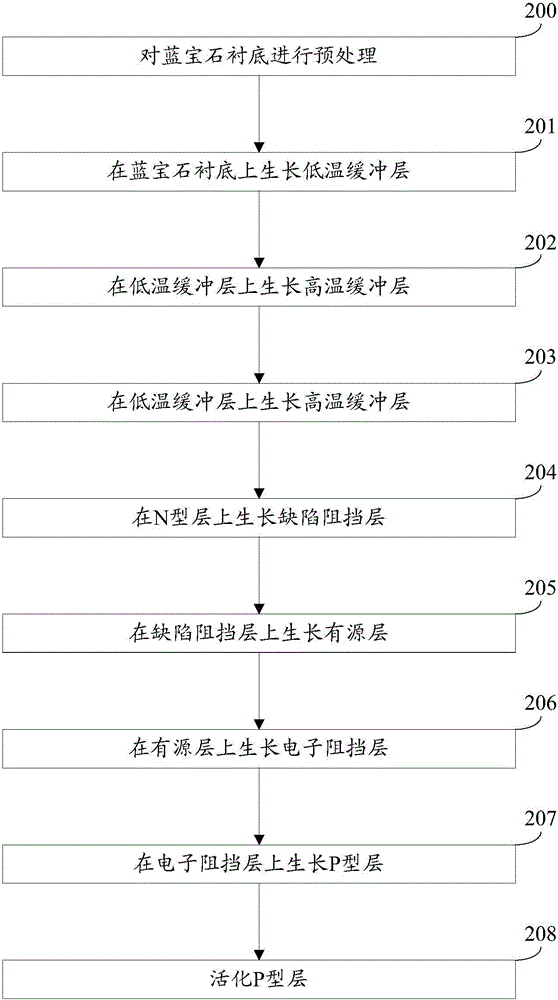
[0055] An embodiment of the present invention provides a method for growing a light-emitting diode epitaxial wafer, which is suitable for growing the light-emitting diode epitaxial wafer provided in Embodiment 1, see figure 2 , the growth method includes:

[0056] Step 200: pretreating the sapphire substrate.

[0057] Specifically, this step 200 may include:

[0058] Under a hydrogen atmosphere, treat the substrate at high temperature for 5-6 minutes.

[0059] Wherein, the temperature of the reaction chamber is 1000-1100° C., and the pressure of the reaction chamber is controlled at 200-500 torr.

[0060] In this embodiment, Veeco K465i or C4MOCVD (Metal Organic Chemical Vapor Deposition, metal organic compound chemical vapor deposition) equipment is used to realize the growth method of LED epitaxial wafers. Using high-purity H 2 (hydrogen), high-purity N 2 (nitrogen), high-purity H 2 and high purity N 2 One of the mixed gases as a carrier gas, high-purity NH 3 As the...


PUM


Abstract

The invention discloses a light-emitting diode epitaxial wafer and a growth method thereof, and belongs to the technical field of semiconductors. The light-emitting diode epitaxial wafer comprises a sapphire substrate, a low-temperature buffer layer, a high-temperature buffer layer, an N-type layer, a defect blocking layer, an active layer, an electron blocking layer and a P-type layer, wherein the defect blocking layer comprises a first sub-layer and a second sub-layer; the first sub-layer comprises first AlGaN layers and GaN layers which are alternately stacked; the second sub-layer comprises second AlGaN layers and third AlGaN layers which are alternately stacked; the Al content in the first AlGaN layers gradually changes along the growth direction of the light-emitting diode epitaxial wafer; and the Al content in the second AlGaN layers and the Al content in the third AlGaN layers remain unchanged, are different and are smaller than that in the first AlGaN layers. The light-emitting diode epitaxial wafer has a blocking effect on extension of defects.

Description

technical field [0001] The invention relates to the technical field of semiconductors, in particular to a light-emitting diode epitaxial wafer and a growth method thereof. Background technique [0002] LED (Light Emitting Diode, Light Emitting Diode) is a semiconductor electronic component that can emit light. As a new type of solid-state lighting source with high efficiency, environmental protection and greenness, LED is rapidly and widely used in fields such as traffic lights, car interior and exterior lights, urban landscape lighting, mobile phone backlight and so on. [0003] Existing LED epitaxial wafers include a sapphire substrate, and a low-temperature buffer layer, a high-temperature buffer layer, an N-type layer, an active layer, and a P-type layer sequentially stacked on the sapphire substrate. Wherein, both the N-type layer and the P-type layer are GaN layers, and the active layer includes alternately stacked InGaN layers and GaN layers. [0004] In the process...

Claims


Application Information

Patent Timeline
Patent Type & Authority Applications(China)
IPC IPC(8): H01L33/12H01L33/00
CPCH01L33/0075H01L33/12
Inventor 姚振从颖胡加辉
Owner HC SEMITEK SUZHOU
Why Eureka
Try Eureka