Light-emitting diode epitaxial wafer and preparation method thereof

A technology for light-emitting diodes and manufacturing methods, applied in electrical components, circuits, semiconductor devices, etc., can solve the problems of reducing the crystal quality of the quantum well layer, reducing the crystal quality of the quantum barrier layer, affecting the crystal integrity of the quantum barrier material, etc. The effect of facilitating electron migration, reducing adverse effects and alleviating adverse effects

Active Publication Date: 2017-10-24
HC SEMITEK ZHEJIANG CO LTD
View PDF6 Cites 9 Cited by
  • Summary
  • Abstract
  • Description
  • Claims
  • Application Information

AI Technical Summary

Problems solved by technology

[0005] If the doping concentration of silicon in the quantum barrier layer is low, it will not be able to reduce line defects and lower the voltage; if the doping concentration of silicon in the quantum barrier layer is high, it will affect the crystalline integrity of the quantum barrier material on the one hand. , reduce the crystal quality of the quantum barrier layer, on the other hand, silicon atoms will diffuse into the quantum well layer, reducing the crystal quality of the quantum well layer, the reduction of the quantum barrier layer and the crystal quality of the quantum barrier layer will affect the luminous efficiency and brightness of the LED, Therefore, it is difficult to reduce line defects and reduce voltage without affecting the luminous brightness

Method used


Image

  • Light-emitting diode epitaxial wafer and preparation method thereof
  • Light-emitting diode epitaxial wafer and preparation method thereof
  • Light-emitting diode epitaxial wafer and preparation method thereof

Examples


Embodiment 1

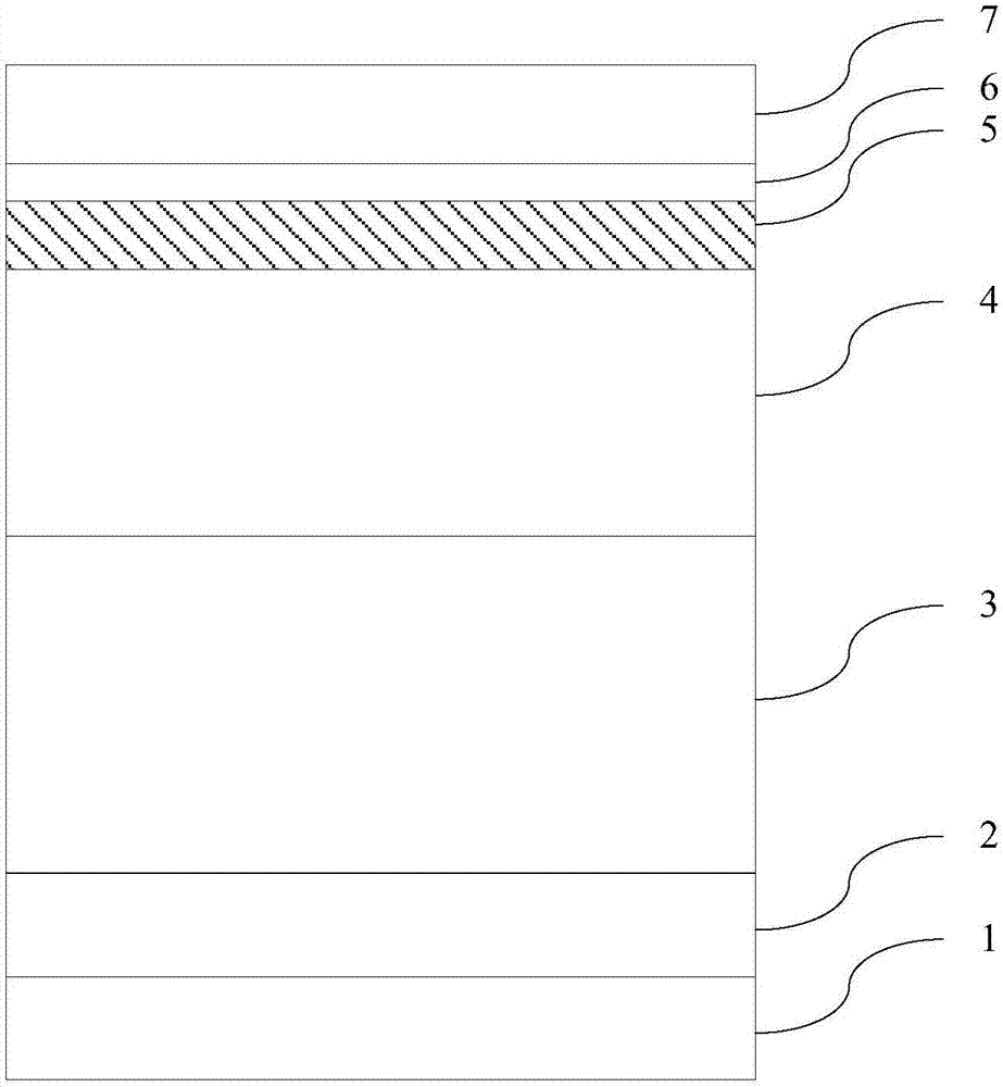
[0033] An embodiment of the present invention provides a light emitting diode epitaxial wafer, see figure 1 , the light-emitting diode epitaxial wafer includes a substrate 1 and a buffer layer 2, an undoped gallium nitride layer 3, an N-type gallium nitride layer 4, a multi-quantum well layer 5, and an electron blocking layer 6 sequentially stacked on the substrate 1 and P-type GaN layer 7 .

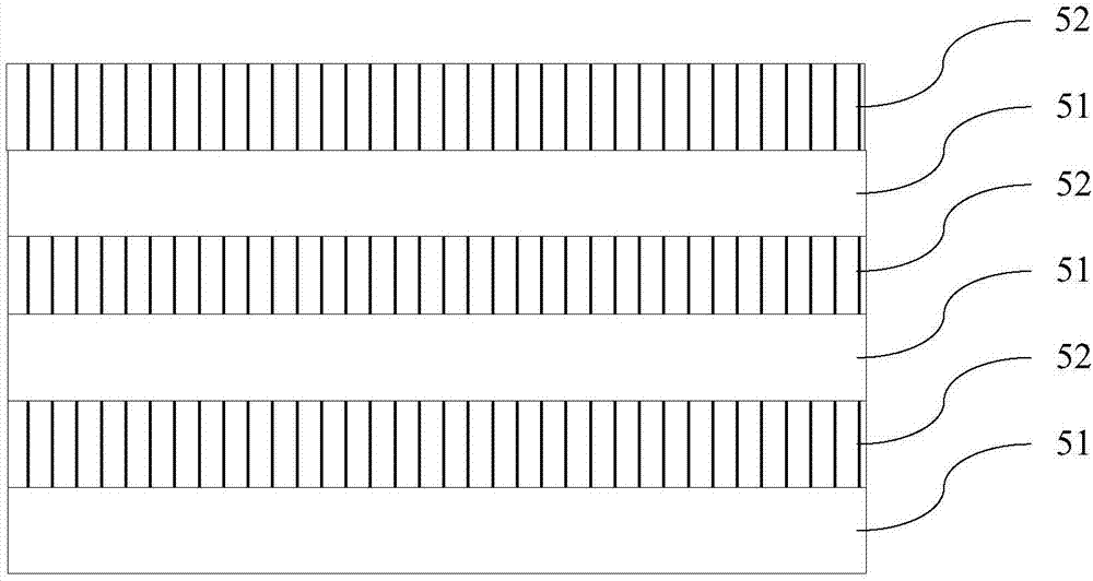
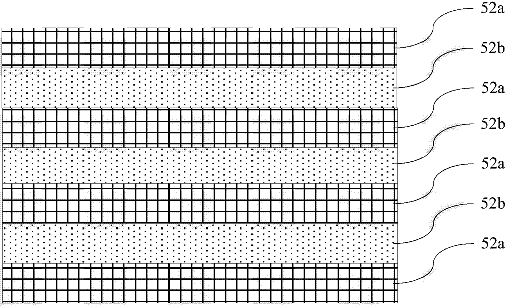
[0034] In this example, see figure 2 , the multi-quantum well layer 5 includes multiple quantum well layers 51 and multiple quantum barrier layers 52, and multiple quantum well layers 51 and multiple quantum barrier layers 52 are stacked alternately. see image 3 , the quantum barrier layer 52 includes (n+1) first sublayers 52a and n second sublayers 52b, n is a positive integer, (n+1) first sublayers 52a and n second sublayers 52b Alternately stacked, the first sub-layer 52a is an undoped gallium nitride layer, and the second sub-layer 52b is a silicon-doped gallium nitride layer. ...

Embodiment 2

[0046] An embodiment of the present invention provides a method for manufacturing a light-emitting diode epitaxial wafer, which is suitable for manufacturing the light-emitting diode epitaxial wafer provided in Embodiment 1, see Figure 4 , the manufacturing method includes:

[0047] Step 201: Provide a substrate.

[0048] Step 202: sequentially growing a buffer layer, an undoped GaN layer, an N-type GaN layer, a multi-quantum well layer, an electron blocking layer and a P-type GaN layer on the substrate.

[0049] In this embodiment, the multi-quantum well layer includes a plurality of quantum well layers and a plurality of quantum barrier layers, the plurality of quantum well layers and the plurality of quantum barrier layers are alternately stacked, and the quantum barrier layer includes (n+1) first sub-layers layer and n second sublayers, n is a positive integer, (n+1) first sublayers and n second sublayers are alternately stacked, the first sublayer is an undoped gallium ...

Embodiment 3

[0061] An embodiment of the present invention provides a method for manufacturing a light-emitting diode epitaxial wafer, and the manufacturing method provided in this embodiment is a specific realization of the manufacturing method provided in Embodiment 2. In this embodiment, Veeco K465i or C4 Metal Organic Chemical Vapor Deposition (English: Metal Organic Chemical Vapor Deposition, abbreviated: MOCVD) equipment is used to realize the manufacture of LED epitaxial wafers. Using high-purity hydrogen (H 2 ) or high-purity nitrogen (N 2 ) or high purity H 2 and high purity N 2 The mixed gas as the carrier gas, high-purity NH 3 As nitrogen source, trimethylgallium (TMGa) and triethylgallium (TEGa) as gallium source, trimethylindium (TMIn) as indium source, trimethylaluminum (TMAl) as aluminum source, silane (SiH4) as N-type dopant, magnesium dicene (CP 2 Mg) as a P-type dopant. The pressure of the reaction chamber is controlled at 100-600 torr.

[0062] Specifically, see ...


PUM


Abstract

The invention discloses a light-emitting diode epitaxial wafer and the preparation method thereof, and belongs to the semiconductor technology field. The epitaxial wafer comprises a substrate, a buffer layer, a non-doped gallium nitride layer, an N-type gallium nitride layer, a multiple quantum well layer, an electron blocking layer, and a P-type gallium nitride layer. The multiple quantum well layer comprises a plurality of quantum well layers and a plurality of quantum barrier layers, which are in an alternately-laminated arrangement. The quantum barrier layers comprise n+1 first sub-layers and n second sub-layers, which are in an alternately-laminated arrangement, and n is a positive integer. The first sub-layers are non-doped gallium nitride layers, and the second sub-layers are gallium nitride layers doped with silicon. The layers doped with the silicon and the non-doped layers are alternately grown, and current expansion is effectively enhanced, and a part of silicon of the gallium nitride layers doped with silicon can permeate into the non-doped gallium nitride layers, and therefore the light-emitting efficiency and the brightness of the LED are guaranteed, and line defects are reduced, and voltage is lowered.

Description

technical field [0001] The invention relates to the technical field of semiconductors, in particular to a light-emitting diode epitaxial wafer and a manufacturing method thereof. Background technique [0002] Light Emitting Diode (English: Light Emitting Diode, referred to as: LED) is a semiconductor electronic component that can emit light. The chip is the core component of the LED, including epitaxial wafers and electrodes arranged on the epitaxial wafers. [0003] The existing LED epitaxial wafer includes a substrate and a buffer layer stacked on the substrate in sequence, an N-type gallium nitride layer, a multiple quantum well (English: Multiple Quantum Well, referred to as: MQW) layer, an electron blocking layer and a P-type nitride layer. gallium layer. Among them, the electrons provided by the N-type gallium nitride layer and the holes provided by the P-type gallium nitride layer are injected into the multi-quantum well layer for radiative recombination and light e...

Claims


Application Information

Patent Timeline
Patent Type & Authority Applications(China)
IPC IPC(8): H01L33/00H01L33/06H01L33/32
CPCH01L33/0066H01L33/0075H01L33/06H01L33/325
Inventor 从颖姚振胡加辉李鹏
Owner HC SEMITEK ZHEJIANG CO LTD
Why Eureka
Try Eureka