T-gate and N-surface GaN/AlGaN fin-type high electron mobility transistor

A high electron mobility, transistor technology, applied in circuits, electrical components, semiconductor devices, etc., can solve the problems of weak short-channel effect suppression, poor two-dimensional electron gas confinement, high ohmic contact resistance, etc. Suppresses short channel effect, improves microwave performance, and reduces ohmic contact resistance

Active Publication Date: 2016-08-31
XIDIAN UNIV
View PDF4 Cites 15 Cited by
  • Summary
  • Abstract
  • Description
  • Claims
  • Application Information

AI Technical Summary

Problems solved by technology

The device uses a Ga-face GaN-based structure. Compared with N-face GaN-based devices, Ga-face GaN-based devices have higher ohmic contact resistance, poor two-dimensional electron gas confinement, and short-channel effects. Inhibition is also weak

Method used


Image

  • T-gate and N-surface GaN/AlGaN fin-type high electron mobility transistor
  • T-gate and N-surface GaN/AlGaN fin-type high electron mobility transistor
  • T-gate and N-surface GaN/AlGaN fin-type high electron mobility transistor

Examples


Embodiment 1

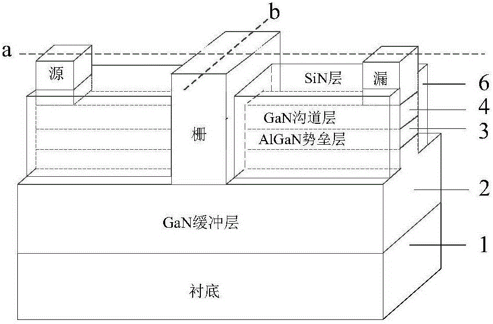
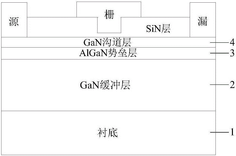
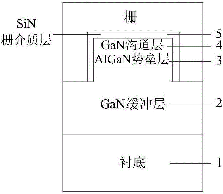
[0028] Example 1: Fabricate a T-gate N-plane GaN / AlGaN fin-type high electron mobility transistor with a fin-type GaN / AlGaN heterojunction width of 2 μm, a T-type gate neck height of 50 nm, and a gate cap height of 100 nm.

[0029] Step 1: growing a buffer layer.

[0030] At a temperature of 680°C and a pressure of 5×10 -3 Under the process condition of Pa, the molecular beam epitaxy MBE equipment is used in Figure 4 (a) An N-face GaN buffer layer with a thickness of 1.5 μm is grown on the sapphire substrate shown in (a).

[0031] Step 2: growing a barrier layer.

[0032] At a temperature of 680°C and a pressure of 5×10 -3 Under the process conditions of Pa, a layer of AlGaN with a thickness of 20nm was first grown on the GaN layer by using molecular beam epitaxy MBE equipment, and the Al composition gradually changed from 5% to 30% from bottom to top; The composition is 30% AlGaN layer.

[0033] Step 3: growing a channel layer.

[0034] At a temperature of 680°C and a ...

Embodiment 2

[0047] Example 2: Fabricate a T-gate N-plane GaN / AlGaN fin-type high electron mobility transistor with a fin-type GaN / AlGaN heterojunction width of 3 μm, a T-type gate neck height of 70 nm, and a gate cap height of 200 nm.

[0048] Step 1: Growth buffer layer.

[0049] On the SiC substrate, a layer of N-face GaN buffer layer with a thickness of 2 μm is grown by molecular beam epitaxy MBE. The growth process conditions are:

[0050] The growth temperature is 680°C and the pressure is 5×10 -3 Pa.

[0051] Step 2: Growing a barrier layer.

[0052] A layer of AlGaN with a thickness of 20nm was grown on the GaN layer by MBE, and the Al composition gradually changed from 5% to 30% from bottom to top; another layer of AlGaN with a thickness of 8nm and an Al composition of 30% was grown layer, the process conditions for its growth are:

[0053] The growth temperature is 680°C and the pressure is 5×10 -3 Pa.

[0054] Step 3: growing a channel layer.

[0055] On the AlGaN layer, ...

Embodiment 3

[0067] Example 3: Fabricate a T-gate N-plane GaN / AlGaN fin-type high electron mobility transistor with a fin-type GaN / AlGaN heterojunction width of 2.5 μm, a T-type gate neck height of 90 nm, and a gate cap height of 250 nm.

[0068] Step A: growing a buffer layer on the substrate.

[0069] Using molecular beam epitaxy MBE equipment at a temperature of 680°C and a pressure of 5×10 -3 Under the process condition of Pa, an N-face GaN buffer layer with a thickness of 2.5 μm is grown on the SiC substrate.

[0070] Step B: growing a barrier layer on the buffer layer.

[0071] Using molecular beam epitaxy MBE equipment at a temperature of 680°C and a pressure of 5×10 -3 Under the process conditions of Pa, a layer of AlGaN with a thickness of 20nm is first grown on the GaN buffer layer, and the Al composition is gradually changed from 5% to 30% from bottom to top, and the thickness of another layer is 5nm, and the Al composition is 30%. AlGaN layer.

[0072] Step C: growing a cha...


PUM


Abstract

The present invention discloses a T-gate and N-surface GaN/AlGaN fin-type high electron mobility transistor. The problems are mainly solved that the maximum oscillating frequency of a current microwave power device is small, the ohmic contact resistor is large and the short channel effect is severe. The transistor comprises from down to up: a substrate (1), a GaN buffer layer (2), a ALGaN barrier layer (3), a GaN channel layer (4), a gate medium layer (5), a passivation layer (6), a source gate electrode and a drain gate electrode. The buffer layer and the channel layer employ N-surface GaN materials; the GaN channel layer and the ALGaN barrier layer form GaN/AlGaN heterojunction; the gate electrode employs T-type gate and is wrapped at two sides and the upper portion of the GaN/AlGaN heterojunction to form a three-dimensional gate structure. The T-gate and N-surface GaN/AlGaN fin-type high electron mobility transistor has good gate-control capability, small resistor and the maximum oscillating frequency, and is able to be a microwave power device with the small size.

Description

technical field [0001] The invention belongs to the technical field of microelectronic devices, in particular to a T-gate N-plane GaN / AlGaN fin-type high electron mobility transistor Fin-HEMT, which can be used for microwave power integrated circuits. Background technique [0002] As a third-generation semiconductor material, GaN material is considered to be an excellent material for making microwave power devices and high-speed devices due to its advantages such as large band gap, high concentration of two-dimensional electron gas 2DEG and high electron saturation velocity. Especially the AlGaN / GaN heterojunction high electron mobility transistor HEMT is widely used in microwave power circuits. [0003] With the shrinking of transistor size, the gate length is getting shorter and shorter, and the short channel effect of traditional high electron mobility transistor HEMT becomes more and more obvious. Ordinary I-type gates have large parasitic capacitance and parasitic resi...

Claims


Application Information

Patent Timeline
Patent Type & Authority Applications(China)
IPC IPC(8): H01L29/778H01L21/336
CPCH01L29/66431H01L29/7783
Inventor 张金风黄旭安阳张进成郝跃
Owner XIDIAN UNIV
Why Eureka
Try Eureka