Mixed-potential low-ppm acetone sensor based on YSZ and MNb2O6 sensitive electrode, and preparation method and application thereof
A hybrid potential type, sensitive electrode technology, applied in the application of diabetes detection, hybrid potential type low-ppm level acetone sensor field, can solve the problem that low ppm acetone detection cannot be realized, achieve good thermal stability and chemical stability, The effect of simple preparation method
- Summary
- Abstract
- Description
- Claims
- Application Information
AI Technical Summary
Problems solved by technology
Method used
Image

Examples
Embodiment 1
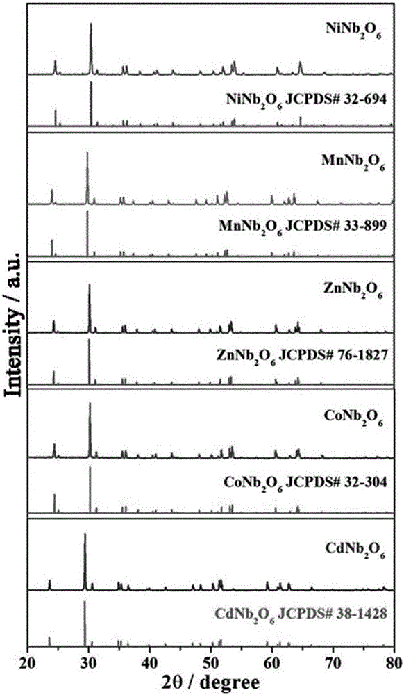
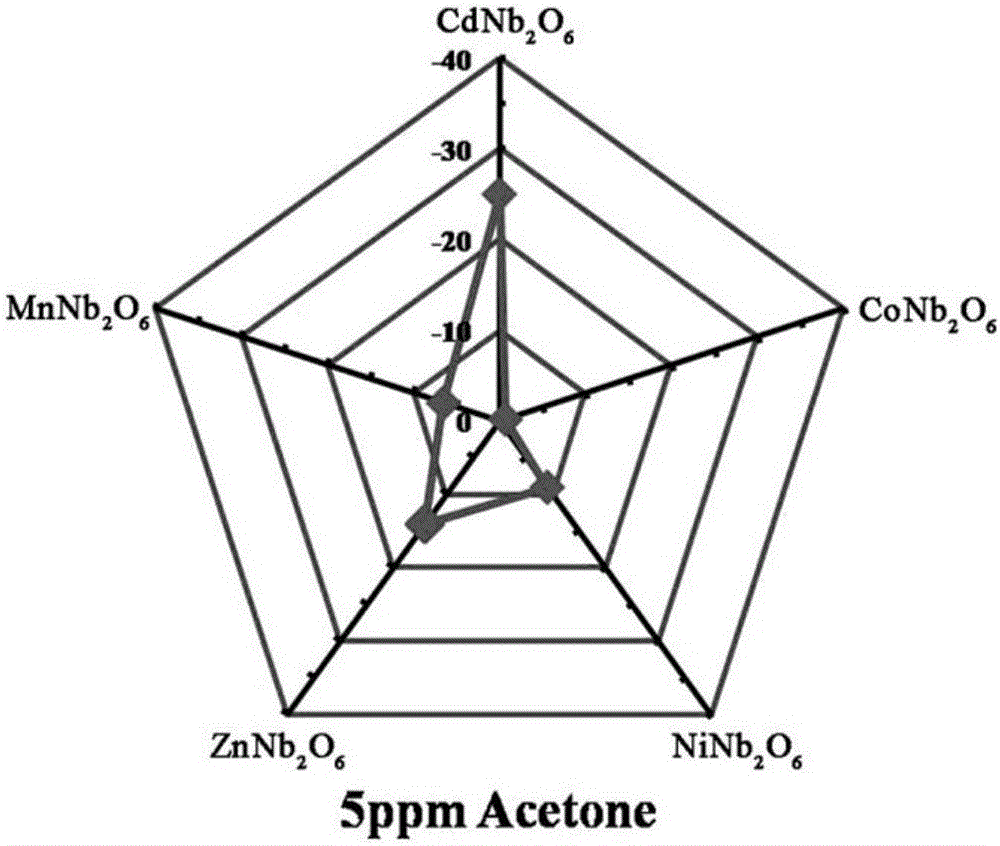
[0036] Preparation of CdNb by Sol-Gel Method 2 o 6 material, the prepared CdNb 2 o 6 As a sensitive electrode material, a YSZ-based hybrid potentiometric sensor was fabricated, and the gas sensitivity of the sensor to acetone was tested. The specific process is as follows:
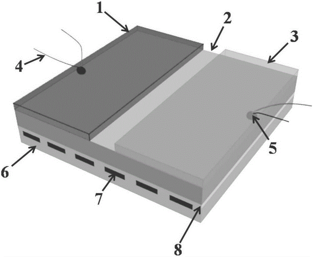
[0037] 1. Make a Pt reference electrode: use Pt slurry to make a Pt reference electrode with a size of 0.5mm×2mm and a thickness of 15μm on one end of the upper surface of the YSZ substrate with a length and width of 2×2mm and a thickness of 0.2mm, and fold it in half with a Pt wire Then stick the electrode lead wire on the middle position of the reference electrode; then bake the YSZ substrate at 100°C for 1.5 hours, and then sinter the YSZ substrate at 1000°C for 1 hour, so as to eliminate the terpineol in the platinum paste, and finally reduce the to room temperature.
[0038] 2. Fabrication of CdNb 2 o 6 Sensitive electrode: first prepare CdNb by sol-gel method 2 o 6 Material. Weigh 3mmol of N...
Embodiment 2
[0044] NiNb 2 o 6 The material is used as a sensitive electrode material to make an acetone sensor. NiNb 2 o 6 The preparation process of the sensitive electrode material and the device fabrication process are the same as in Example 1.
Embodiment 3
[0046] ZnNb 2 o 6 The material is used as a sensitive electrode material to make an acetone sensor. ZnNb 2 o 6 The preparation process of the sensitive electrode material and the device fabrication process are the same as in Example 1.
PUM
 Abstract
Description
Claims
Application Information
 - R&D
- Intellectual Property
- Life Sciences
- Materials
- Tech Scout
- Unparalleled Data Quality
- Higher Quality Content
- 60% Fewer Hallucinations
Browse by: Latest US Patents, China's latest patents, Technical Efficacy Thesaurus, Application Domain, Technology Topic, Popular Technical Reports.
© 2025 PatSnap. All rights reserved.Legal|Privacy policy|Modern Slavery Act Transparency Statement|Sitemap|About US| Contact US: help@patsnap.com