Eureka AIR delivers breakthrough ideas for toughest innovation challenges, trusted by R&D personnel around the world.

Trench-gate power MOSFET and manufacturing method

A trench gate and power technology is applied in the manufacture of trench gate power MOSFETs and in the field of trench gate power MOSFETs. The effect of uniform passage, increased breakdown voltage, and improved UIS shock resistance

Active Publication Date: 2016-09-07
SHANGHAI HUAHONG GRACE SEMICON MFG CORP
View PDF6 Cites 6 Cited by
  • Summary
  • Abstract
  • Description
  • Claims
  • Application Information

AI Technical Summary

Problems solved by technology

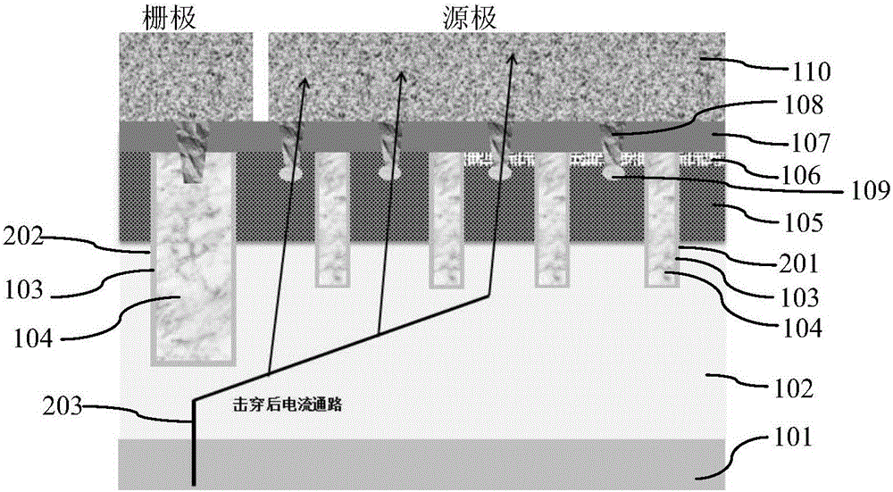
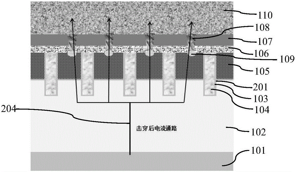
However, in the existing structure, because the depth of the trench 202 is deep, the devices are edge breakdown, and the poor uniformity of the distribution of the current path after the edge breakdown is likely to lead to the opening of the parasitic NPN transistor, thereby reducing the anti-abnormality of the device. Unclamped Inductive Switching (UIS) impact capability, UIS impact resistance is the ability of the device to load energy under avalanche breakdown

Method used


Image

  • Trench-gate power MOSFET and manufacturing method
  • Trench-gate power MOSFET and manufacturing method
  • Trench-gate power MOSFET and manufacturing method

Examples


Embodiment Construction

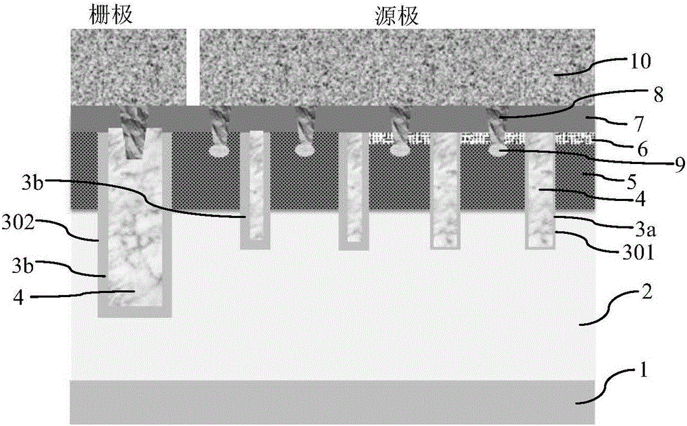
[0056] like figure 2 As shown, it is a schematic structural diagram of the trench gate power MOSFET of the embodiment of the present invention; the trench gate power MOSFET of the embodiment of the present invention includes an inner region and an edge region, and the inner region is the conduction region of the trench gate power MOSFET, which consists of multiple The original cell, that is, the unit structure (cell) is periodically arranged; the edge area is located at the edge of the conduction area, and is used to lead out the gate structure of each original cell in the conduction area; in the inner area A drift region 2 of the first conductivity type and a body region 5 of the second conductivity type are formed in the edge region, and the body region 5 is located on the surface of the drift region 2; the drift region 2 is formed on the semiconductor substrate Bottom 1 surface. Preferably, the semiconductor substrate 1 is a silicon substrate.

[0057] A first groove 301...


PUM


Abstract

The invention discloses a trench-gate power MOSFET. The thicknesses of first gate dielectric layers in trenches in an internal region and second gate dielectric layers in the trenches in an edge region are independently set; and the thicknesses of the second gate dielectric layers are greater than those of the first gate dielectric layers. A threshold voltage of a device is adjusted through the thicknesses of the first gate dielectric layers; the electric field strength in the edge region is reduced and the voltage-withstand capability of the edge region is improved by increasing the thicknesses of the second gate dielectric layers; breakdown of the device is demanded in the internal region; and the impact resistance of the device is improved. The invention further discloses a manufacturing method of the trench-gate power MOSFET. The breakdown voltage of the device can be improved; and the anti-UIS impact ability of the device is improved. Independent adjustment of the thicknesses of the first gate dielectric layers and the second gate dielectric layers is achieved by source injection lithography; and an extra lithography process is not needed, so that the process cost is not increased.

Description

technical field [0001] The invention relates to the field of manufacturing semiconductor integrated circuits, in particular to a trench gate power MOSFET. The invention also relates to a method for manufacturing the trench gate power MOSFET. Background technique [0002] like Figure 1A Shown is a schematic diagram of the structure of the edge region of the existing trench gate power MOSFET; as Figure 1B Shown is a schematic diagram of the structure of the internal region of the existing trench gate power MOSFET; the device structure includes: [0003] A semiconductor substrate such as a silicon substrate 101 is formed on an epitaxial layer 102 on the surface of the semiconductor substrate 101 , and the drift region is composed of the epitaxial layer 102 . [0004] The groove of the trench gate is formed in the epitaxial layer 102, wherein the grooves in the inner region are marked with a mark 201, and there is a wider groove 202 in the edge region, that is, the width of ...

Claims


Application Information

Patent Timeline
Patent Type & Authority Applications(China)
IPC IPC(8): H01L29/78H01L21/336H01L29/423
CPCH01L29/4236H01L29/42368H01L29/66477H01L29/78
Inventor 柯行飞
Owner SHANGHAI HUAHONG GRACE SEMICON MFG CORP
Why Eureka
Eureka Blog
Learn More