
Etchant composition and manufacturing method of an array substrate for liquid crystal display

A composition and etchant technology, applied in the directions of surface etching compositions, chemical instruments and methods, semiconductor/solid-state device manufacturing, etc., can solve the problem of low etching rate variation with time, unfavorable process limitations, inability to etch amorphous silicon problems such as thin layers to achieve the effect of reducing processing time and manufacturing costs

Inactive Publication Date: 2016-10-12
DONGWOO FINE CHEM CO LTD
View PDF0 Cites 4 Cited by
  • Summary
  • Abstract
  • Description
  • Claims
  • Application Information

AI Technical Summary

Problems solved by technology

When the copper / titanium layer is etched using the above etchant, the gate line or pattern is preserved, moreover, a high etch rate and low time variation can be obtained, but it cannot etch the thin layer of amorphous silicon (n+a-Si: H), disadvantageously incurs process limitations which require an additional dry etch process

Method used


Image

  • Etchant composition and manufacturing method of an array substrate for liquid crystal display
  • Etchant composition and manufacturing method of an array substrate for liquid crystal display
  • Etchant composition and manufacturing method of an array substrate for liquid crystal display

Examples


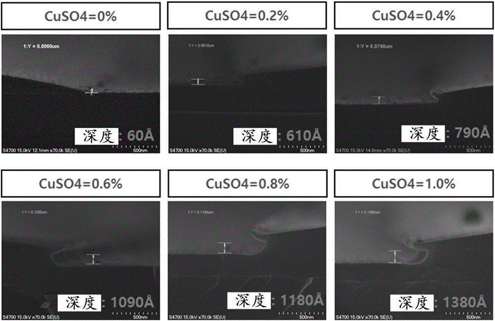
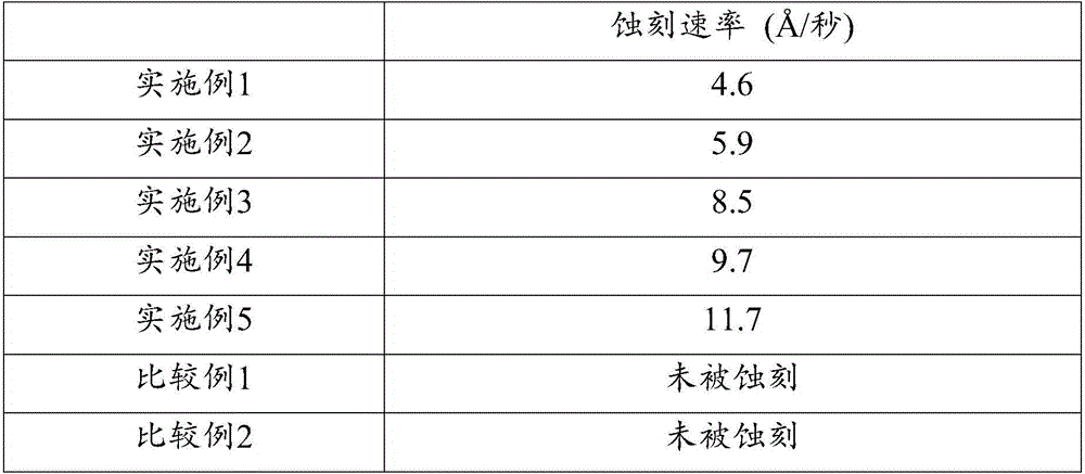
Embodiment 1-5 and comparative example 1 and 2

[0036] Examples 1-5 and Comparative Examples 1 and 2: Preparation of etchant compositions

[0037] An etchant composition was prepared using the ingredients in the amounts (wt %) shown in Table 1 below.

[0038] [Table 1]

[0039]

APS

AF

HNO 3

ATZ

p-TSA

A.A.

AcOH

CuSO 4

water

Example 1

15

0.7

3

1.2

3.0

2.5

8.0

0.2

margin

Example 2

15

0.7

3

1.2

3.0

2.5

8.0

0.4

margin

Example 3

15

0.7

3

1.2

3.0

2.5

8.0

0.6

margin

Example 4

15

0.7

3

1.2

3.0

2.5

8.0

0.8

margin

Example 5

15

0.7

3

1.2

3.0

2.5

8.0

1.0

margin

Comparative example 1

15

0.7

3

1.2

3.0

2.5

8.0

-

margin

Comparative example 2

15

0.7

3

1.2

0.0

2.5

8.0

-

margin

[0040] *APS: Ammonium persulfate

[0041] *AF: Ammonium fluoride ...


PUM


Abstract

The invention discloses an etchant composition and a manufacturing method of an array substrate for liquid crystal display. The etchant composition can perform multilayer wet-method etching to at least one of an amorphous Silicon (n+a < Si:H) or a metal oxide layer, and at least one of a copper layer and a copper alloy layer and at least one of a titanium layer and a titanium alloy layer, thereby reducing total processing time and manufacturing cost.

Description

technical field [0001] The present invention relates to an etchant composition and a method of manufacturing an array substrate for a liquid crystal display. Background technique [0002] Electronic circuits for driving semiconductor devices or flat panel displays are generally exemplified by thin film transistors (TFTs). The fabrication of TFT generally involves forming a metal layer for gate lines and data lines on a substrate, forming a photoresist on selected areas of the metal layer and using the photoresist as a mask Etch the metal layer. [0003] Generally, materials for gate lines and data lines include: a copper single layer or a copper alloy layer containing copper having high electrical conductivity and low resistance, and a metal oxide having excellent interfacial adhesion with the above copper layer layer. In order to improve the performance of TFTs, the metal oxide layer is currently made of gallium oxide, indium oxide, zinc oxide or a mixture thereof. [0...

Claims


Application Information

Patent Timeline
Patent Type & Authority Applications(China)
IPC IPC(8): C09K13/08C23F1/18C23F1/26H01L21/77
CPCH01L21/77C09K13/08C23F1/18C23F1/26C23F1/02
Inventor 刘仁浩南基龙李承洙
Owner DONGWOO FINE CHEM CO LTD
Learn More