A method for passivating the front and side walls of a discrete device chip

A technology of discrete devices and chips, which is applied in the passivation of chips, the front and side wall passivation of discrete device chips, can solve the problems of high manufacturing cost and long manufacturing cycle, and achieve short manufacturing cycle, good side wall protection, and process stable effect

Active Publication Date: 2020-02-07
CHINA RESOURCES MICROELECTRONICS (CHONGQING) CO LTD
View PDF5 Cites 0 Cited by
  • Summary
  • Abstract
  • Description
  • Claims
  • Application Information

AI Technical Summary

Problems solved by technology

[0005] In view of the shortcomings of the prior art described above, the purpose of the present invention is to provide a method for passivating the front and side walls of a discrete device chip, which is used to solve the problem of high manufacturing cost and long manufacturing cycle of chip passivation in the prior art. question

Method used


Image

  • A method for passivating the front and side walls of a discrete device chip
  • A method for passivating the front and side walls of a discrete device chip
  • A method for passivating the front and side walls of a discrete device chip

Examples


Embodiment 1

[0029] Such as Figure 1 to Figure 7 As shown, the present embodiment provides a method for passivating the front and side walls of a discrete device chip, and the passivation method includes the steps of:

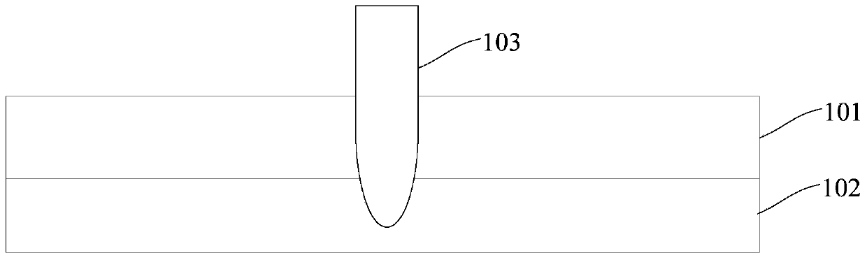
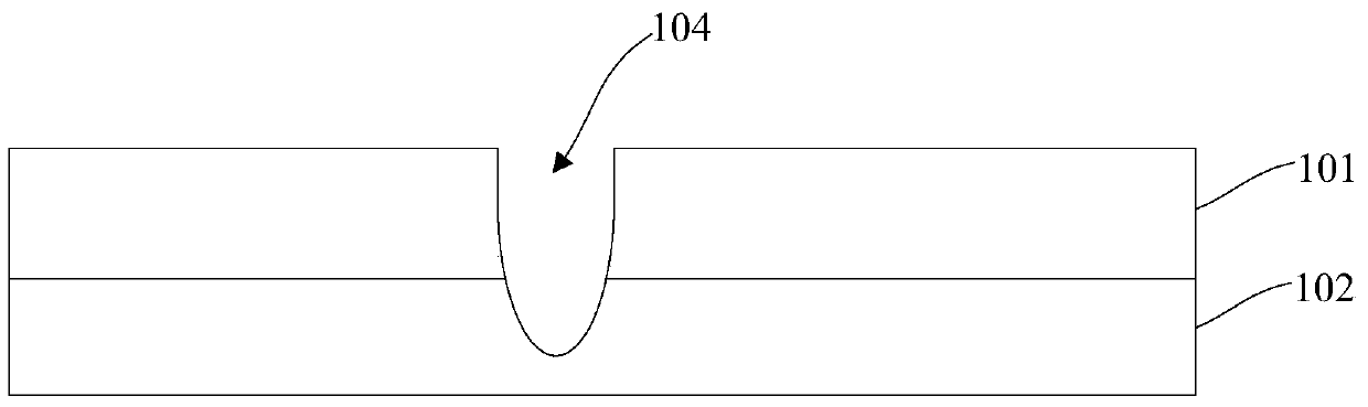
[0030] Such as Figure 1 ~ Figure 2 As shown, step 1) is first performed, providing a chip wafer 101 , and cutting the chip wafer 101 to form a plurality of dicing lines 104 .

[0031] As an example, the discrete device includes a Schottky barrier diode, that is, the chip wafer 101 is a wafer including a plurality of Schottky barrier diode chips.

[0032] As an example, before dicing, a step is further included: bonding the back of the chip wafer 101 to an adhesive layer 102 , specifically, the adhesive layer 102 can be selected as a blue film, a bandage, or the like.

[0033] As an example, a dicing knife 103 is used to mechanically cut the chip wafer 101 to form a plurality of dicing lines 104 . The dicing line 104 can completely pass through the chip wafer 101 or leav...

Embodiment 2

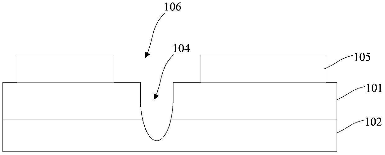
[0044] This embodiment provides a method for passivating the front and side walls of a discrete device chip, the basic steps of which are as in Embodiment 1, the difference from Embodiment 1 is that the screen 105 is to be passivated on the front of the chip wafer 101 There are openings 106 at the position of the layer, step 3) attaching a passivation material 107 at the position where the passivation layer is to be prepared.

[0045] Visible, discrete device chip front and sidewall passivation method of the present invention is not only applicable to the sidewall passivation layer making of chip, and is also applicable to the passivation layer making of chip front or other positions, simplifies the chip front passivation layer production. production process. The invention has a wider scope of application and has wider application prospects in the field of semiconductor manufacturing.

[0046] As mentioned above, the method for passivating the front and side walls of the disc...


PUM


Abstract

The invention provides a passivating method for the front side and side walls of a discrete device chip. The method comprises: step 1), providing a chip wafer and cutting the chip wafer to form multiple cut channels; step 2), providing a screen printing plate which is provided with holes matched with the cut channel pattern of the chip wafer, wherein the screen printing plate and the chip wafer are aligned and fixed; and step 3), based on the screen printing plate, allowing a passivating material to go through the holes and then get attached to the side walls of the cut channels. According to the passivating method, with adoption of a solder resist ink spraying technology, in combination with screen printing plate pattern design for manufacturing, through UV curing, thermocuring and the like, the passivating protection of the front side and side walls of the discrete device chip, especially a SBD product is realized, short circuit caused by draining material during lead bonding of unpacked chip packaging of a chip can be prevented, side wall protection of an electronic chip can be realized well. Compared with a traditional discrete device manufacturing process, the method has the features of low price, stable process, excellent and reliable performance, short manufacturing period, flexible design and the like.

Description

technical field [0001] The invention relates to a passivation method for a chip, which belongs to the field of semiconductor manufacturing, in particular to a passivation method for the front and side walls of a discrete device chip. Background technique [0002] With the continuous development of semiconductor technology, power devices, as a new type of device, are widely used in fields such as disk drives and automotive electronics. Power devices need to be able to withstand large voltage, current and power loads. However, existing devices such as MOS transistors cannot meet the above requirements. Therefore, in order to meet the needs of applications, various power devices have become the focus of attention. [0003] Schottky barrier diodes (SBD) generally use Schottky metals (titanium, nickel, cobalt, chromium, platinum, etc.) properties of metal-semiconductor devices. Because there are a large number of electrons in the N-type semiconductor and only a small amount of...

Claims


Application Information

Patent Timeline
Patent Type & Authority Patents(China)
IPC IPC(8): H01L21/56H01L23/31
CPCH01L21/56H01L23/3171H01L2224/48091H01L2924/00014
Inventor 郑晨焱张小辛粟笛
Owner CHINA RESOURCES MICROELECTRONICS (CHONGQING) CO LTD
Why Eureka
Try Eureka