Digital correction method for array analog to digital converter of high-performance CMOS image sensor

An image sensor and analog-to-digital converter technology, which is applied in image communication, color TV components, and TV system components to save chip area, reduce mismatch problems, and save area.

Active Publication Date: 2016-10-12
JILIN UNIV
View PDF10 Cites 10 Cited by
  • Summary
  • Abstract
  • Description
  • Claims
  • Application Information

AI Technical Summary

Problems solved by technology

Although the traditional SAR ADC also needs N operations to get the final conversion result, its power consumpti

Method used


Image

  • Digital correction method for array analog to digital converter of high-performance CMOS image sensor
  • Digital correction method for array analog to digital converter of high-performance CMOS image sensor
  • Digital correction method for array analog to digital converter of high-performance CMOS image sensor

Examples


Embodiment 1

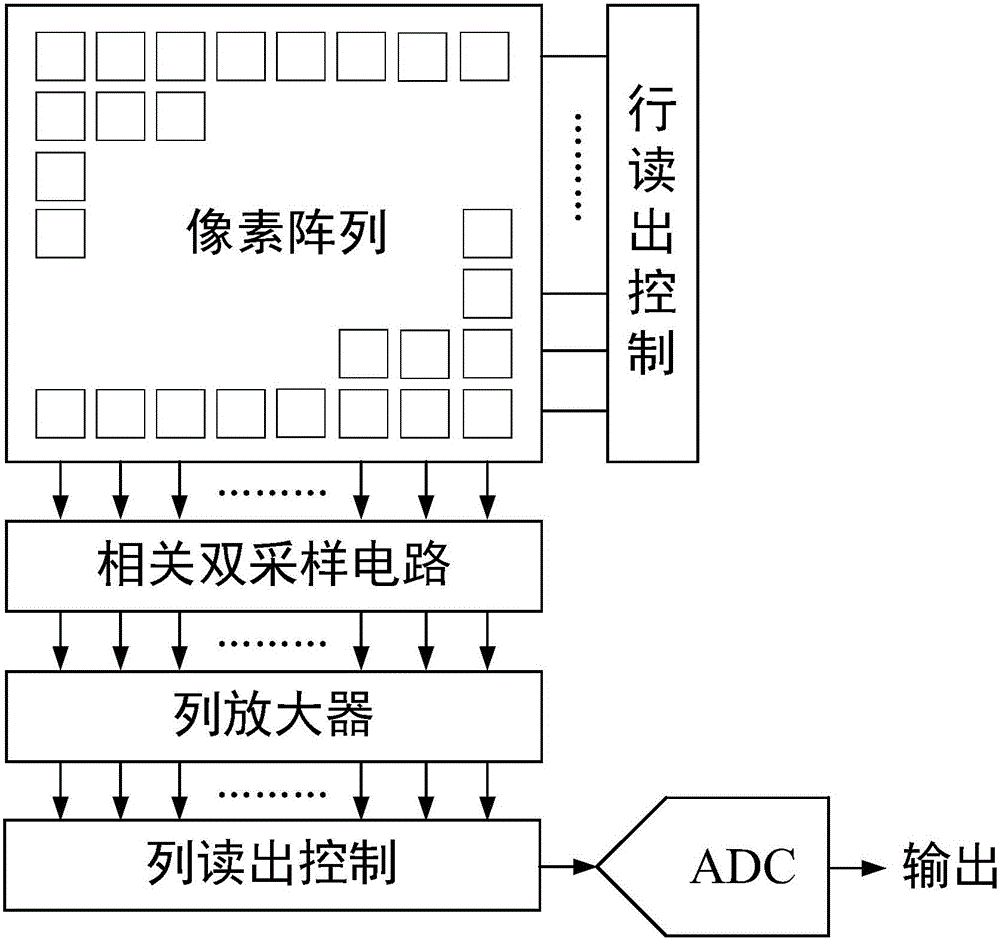
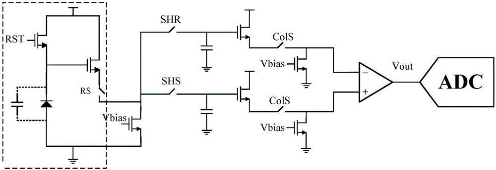
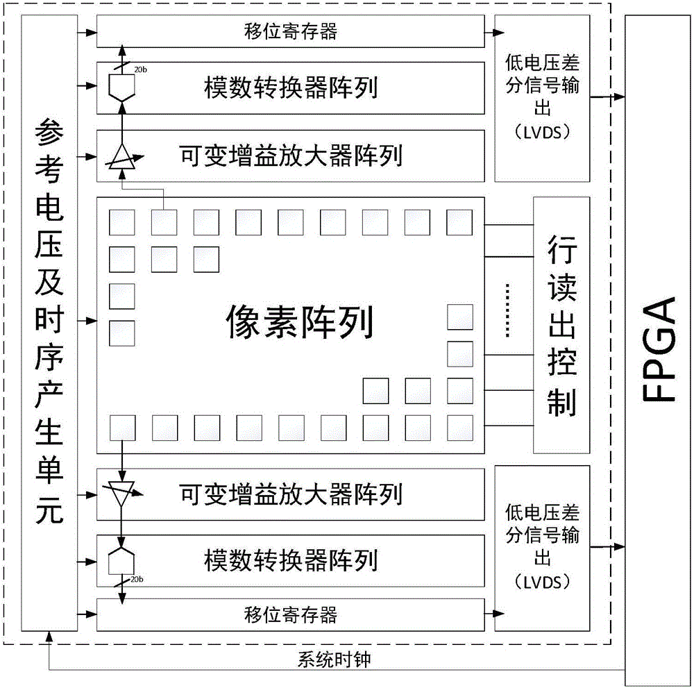
[0042] The digital correction method of the high-performance CMOS image sensor array analog-to-digital converter is as follows: N-channel ADCs on the CIS chip are arranged in an array. During normal operation, the data strobe (MUX) connects the sensor output with the ADC input. In the calibration stage, the data strobe connects the calibration signal to the ADC input, and the ADC output is connected to the off-chip in-circuit system programming (ISP) chip of the CIS through a low-voltage differential signal output (LVDS) high-speed interface. During the digital calibration process, the ADC The output first performs data recovery operation through the bit weight adjustment circuit, and then inputs it into the digital correction engine for correction operation, feeds back the corrected data to the bit weight adjustment circuit for bit weight correction, and then outputs the corrected data to the subsequent image signal processing module The circuit completes the following routine...


PUM


Abstract

The invention belongs to the field of semiconductor image sensing, and specifically relates to a digital correction method for an array analog to digital converter of a high-performance CMOS image sensor. The invention provides an algorithm based on a multi-way collaborative digital correction technology. In particular, for the features that the number of the ADCs in the array ADC of the CIS is high, the area of a single ADC is very small and capacitance mismatch is high, according to the algorithm, an analog to digital converter array which is applied to the CIS and is realized by matching with the algorithm fully is designed. A low working voltage of 1.8V is employed in the integral design. The pixel voltage of the image sensor passes through a variable gain amplifier (VGA), then is directly sent to the analog to the digital converter (ADC) array for conversion, and then is sent to a digital correction engine for calculation. The array analog to digital converter applied to the CMOS image sensor is taken as an integral system. The mismatch problem due to the fact that the area of the single analog to digital converter of the array analog to digital converter is small is reduced to a great extent. According to the multi-way collaborative digital correction technology of the array analog to digital converter applied to the CMOS image sensor provided by the invention, the integral performance of the array analog to digital converter can be effectively improved.

Description

technical field [0001] The invention belongs to the field of semiconductor image sensing, and in particular relates to a multi-channel cooperative digital correction method for an array analog-to-digital converter chip of a high-performance CMOS image sensor. Background technique [0002] In recent years, CMOS image sensor (CIS) has achieved great success in both consumer electronics and professional fields. Except for very special applications, it has basically replaced the traditional CCD image sensor. The integrated analog-to-digital converter (ADC) array on the CIS chip helps to improve system integration, enhance the signal-to-noise ratio and signal anti-interference ability. At present, people have put forward higher requirements for CIS, mainly in the following three aspects: [0003] (1) High resolution. The resolution of the early CIS is VGA (640×480) level; at present, mainstream HDTV (1080p) requires a single-chip color CIS resolution of 9 million pixels, 4K lev...

Claims


Application Information

Patent Timeline
IPC IPC(8): H04N5/3745H04N5/378H04N5/357
CPCH04N25/60H04N25/772H04N25/75
Inventor 常玉春刘明杭李海彬杨姝陈佳俊李亮
Owner JILIN UNIV
Why Eureka
Try Eureka