

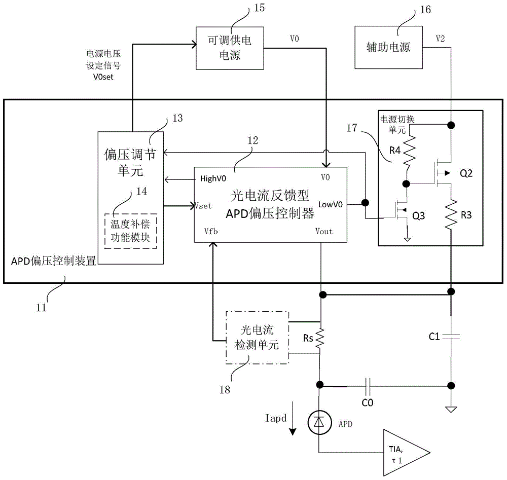
Low-power consumption APD bias controller, bias control method, and photoelectric receiver
A bias voltage control and photocurrent technology, applied in the field of optical communication, can solve the problems of APD/TIA overload damage, photocurrent overload, TIA bit error, etc., and achieve the effect of improving sensitivity and high signal-to-noise ratio.
- Summary
- Abstract
- Description
- Claims
- Application Information
AI Technical Summary
Problems solved by technology
Method used
Image

Examples
Embodiment 1
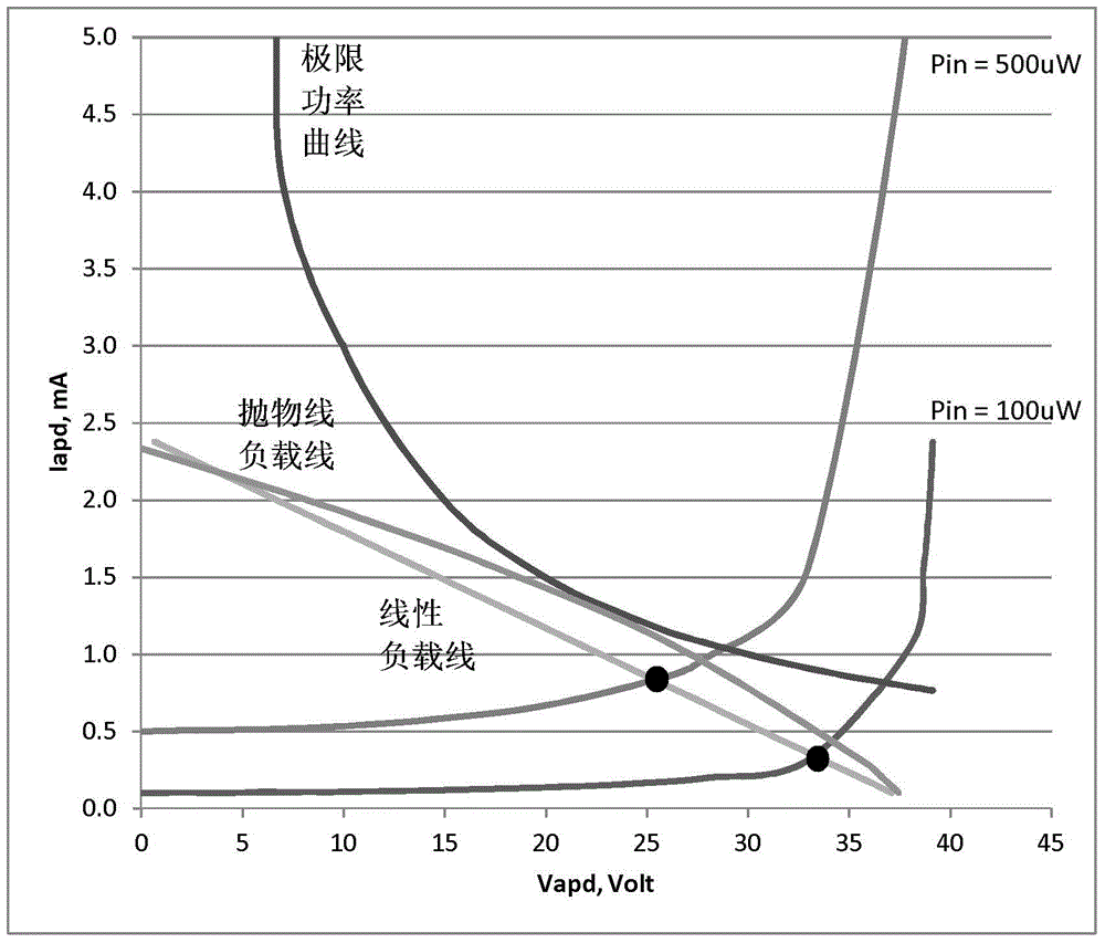
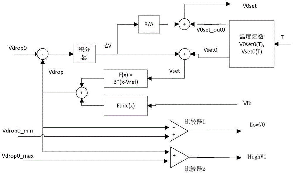
[0097] Assume an APD, Vbr=+40V, n=2. It is further assumed that Vin=+0.8V, Vs is negligible, the sampling circuit gain (Rs*Gs) is 0.5k ohm, and the APD responsivity η=1mA / mW. Set V0=+40V, and select func(x) as a linear function, namely
[0098] func(Vfb)=32*Vfb+0.5=16e3*Iapd+0.5 (8)
[0099] Vapd=40–0.8–Vdrop=38.7–16k*Iapd (9)
[0100] Such as Figure 1aAs shown, we can draw the APD load curve (here a straight line) on the I-V diagram according to formula 9; on the other hand, according to formula 3, we can draw the APD operating characteristic curves with input optical power of 100uW and 500uW respectively. On the I-V diagram, the intersection of the APD operating characteristic curve and the load curve is the APD bias voltage and photocurrent corresponding to the input optical power.
[0101] Assuming that the sensitivity Pin=3.8uW, according to the I-V diagram, it can be obtained that Iapd=40uA at this time, according to formulas 8 and 9, Vdrop=1.14V, Vapd=38.06V, accor...
Embodiment 2
[0157] Continue to use the characteristic parameters and circuit parameters of the APD in Embodiment 1, and assume that the sensitivity index is 3.8uW, func (x) is set to be determined by formula 5 as a linear increasing function, i.e. func (Vfb)=16k*Iapd+0.5, and set B =32, Vset0=Vref=+1.25V, A=32, Vset_out0=V0 / A=1.25V. It is further assumed that Vdrop0=0.82V, Vdrop_min=Vdrop_extreme=0.5V, Vdrop_max=1.14V. The following describes the working mode of the Vdrop control loop when the input optical power increases from the sensitivity point of 3.8uW (corresponding to Iapd=40uA) to +1.94mW (corresponding to Iapd=2mA).
[0158] Calculated according to Example 1, when the input optical power is 3.8uW, if Vdrop is not controlled, according to Figure 1a The load curve and characteristic curve shown are Iapd=40uA, Vapd=38.06V, Vdrop=1.14V. After starting the Vdrop control loop, since Vdrop is greater than its target value of 0.82V, the error integrator gradually increases ΔV in the ...
Embodiment 3
[0210] Assume that the APD characteristic parameters, circuit parameters and Vdrop function are set the same as those in Embodiment 2. Configure R3=16k ohm, according to the aforementioned calibration steps and formulas 22 and 25, it can be obtained: V0set_opt=1.25V, C=0.5V, V2=40-0.5=39.5V. Further assume that the stabilization time of the Vdrop control loop is about 500ms, the current input optical power Pin=1.95mW, Iapd is stable at 2mA, the Vdrop control loop is stable, Vdrop=0.82V, V0=8.32V. The table below describes a change process of the working state of the circuit when the optical power is reduced to the sensitivity point Pin=3.8uW within 10us.
[0211] Table 1:
[0212]
[0213] According to the APD bias voltage control method provided by the present invention, the APD bias voltage controller and the bias voltage adjustment device can be conveniently designed by using hardware circuits or software algorithms or a combination of software and hardware.
[0214] ...
PUM
 Abstract
Description
Claims
Application Information