

Novel method for preparing single-layer MoS2
A new method, single-layer technology, applied in the field of materials, can solve the problems of low repeatability and inability to guarantee the preparation of single-layer MoS2, and achieve the effects of improved repeatability, short preparation cycle and low cost
- Summary
- Abstract
- Description
- Claims
- Application Information
AI Technical Summary
Problems solved by technology
Method used
Image

Examples
Embodiment 1
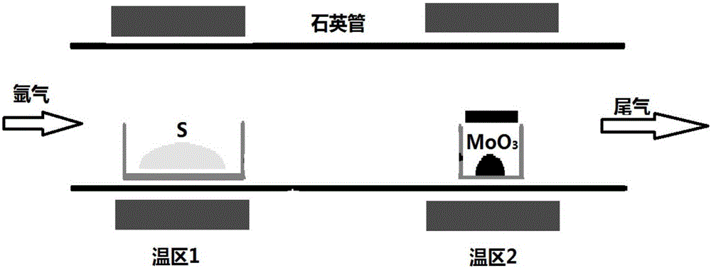
[0052] Step (1). SiO 2 (300nm) / Si sheet cut into 1cm 2 Small square blocks serve as substrates.
[0053] Step (2). Ultrasonic cleaning of the substrate obtained in step (1) with deionized water at room temperature for 10 minutes.
[0054] Step (3). Ultrasonic cleaning of the substrate obtained in step (2) with AR, 99.7% absolute ethanol solution at room temperature for 10 minutes.
[0055] Step (4). Ultrasonic cleaning of the substrate obtained in step (3) with deionized water at room temperature for 10 minutes.
[0056] Step (5). Ultrasonic cleaning of the substrate obtained in step (4) with 30% hydrogen peroxide at normal temperature for 10 minutes.
[0057] Step (6). Ultrasonic cleaning of the substrate obtained in step (5) with deionized water at room temperature for 10 minutes.
[0058] Step (7). Blow dry the substrate obtained in step (6), and then set the speed of the homogenizer at a low speed of 2000 rpm and a high speed of 8000 rpm, and control the spin coating t...
Embodiment 2
[0066] Step (1). SiO 2 (300nm) / Si sheet cut into 1cm 2 Small square blocks serve as substrates.
[0067] Step (2). Ultrasonic cleaning of the substrate obtained in step (1) with deionized water at room temperature for 10 minutes.
[0068] Step (3). Ultrasonic cleaning of the substrate obtained in step (2) with AR, 99.7% absolute ethanol solution at room temperature for 10 minutes.
[0069] Step (4). Ultrasonic cleaning of the substrate obtained in step (3) with deionized water at room temperature for 10 minutes.
[0070] Step (5). Ultrasonic cleaning of the substrate obtained in step (4) with 30% hydrogen peroxide at normal temperature for 10 minutes.
[0071] Step (6). Ultrasonic cleaning of the substrate obtained in step (5) with deionized water at room temperature for 10 minutes.
[0072] Step (7). Dry the substrate obtained in step (6), then soak the bottom of the substrate into the graphene oxide quantum dot solution, then take out the substrate by pulling method, and...
Embodiment 4
[0077] Step (1). SiO 2 (300nm) / Si sheet cut into 1cm 2 A small square block serves as a substrate.
[0078] Step (2). Ultrasonic cleaning of the substrate obtained in step (1) with deionized water at room temperature for 10 minutes.
[0079] Step (3). Ultrasonic cleaning of the substrate obtained in step (2) with AR, 99.7% absolute ethanol solution at room temperature for 10 minutes.
[0080] Step (4). Ultrasonic cleaning of the substrate obtained in step (3) with deionized water at room temperature for 10 minutes.
[0081] Step (5). Ultrasonic cleaning of the substrate obtained in step (4) with 30% hydrogen peroxide at normal temperature for 10 minutes.
[0082] Step (6). Ultrasonic cleaning of the substrate obtained in step (5) with deionized water at room temperature for 10 minutes.
[0083] Step (7). Dry the substrate obtained in step (6), then set the speed of the glue homogenizer to 1000 rpm at a low speed and 7000 rpm at a high speed, and control the spin coating ti...
PUM
| Property | Measurement | Unit |
|---|---|---|
| Wavelength | aaaaa | aaaaa |
Abstract
Description
Claims
Application Information