RTD diode of indium gallium nitride emitting electrode ohmic contact layer and manufacturing method thereof

An ohmic contact layer and manufacturing method technology, applied in the field of electronics, can solve the problems of In precipitation, reduce output power, large leakage, etc., and achieve the effects of high peak current, large output power, and small leakage

Active Publication Date: 2016-10-26
XIDIAN UNIV
View PDF3 Cites 13 Cited by
  • Summary
  • Abstract
  • Description
  • Claims
  • Application Information

AI Technical Summary

Problems solved by technology

The disadvantage of this method is that because the two-dimensional electron gas concentration at the AlAs / InGaAs interface is not high and the mobility is not high, the operating frequency and output power cannot meet the output requirements of terahertz devices.
The disadvantage of this method is that due to the negative polarized charge between the second GaN isolation layer and the second InGaN sub-quantum well layer, electron depletion will occur, thereby reducing the peak current and reducing the output power; on InGaN Growing GaN requires a high-temperature process, which may cause In precipitation and large leakage

Method used


Image

  • RTD diode of indium gallium nitride emitting electrode ohmic contact layer and manufacturing method thereof
  • RTD diode of indium gallium nitride emitting electrode ohmic contact layer and manufacturing method thereof
  • RTD diode of indium gallium nitride emitting electrode ohmic contact layer and manufacturing method thereof

Examples


Embodiment 1

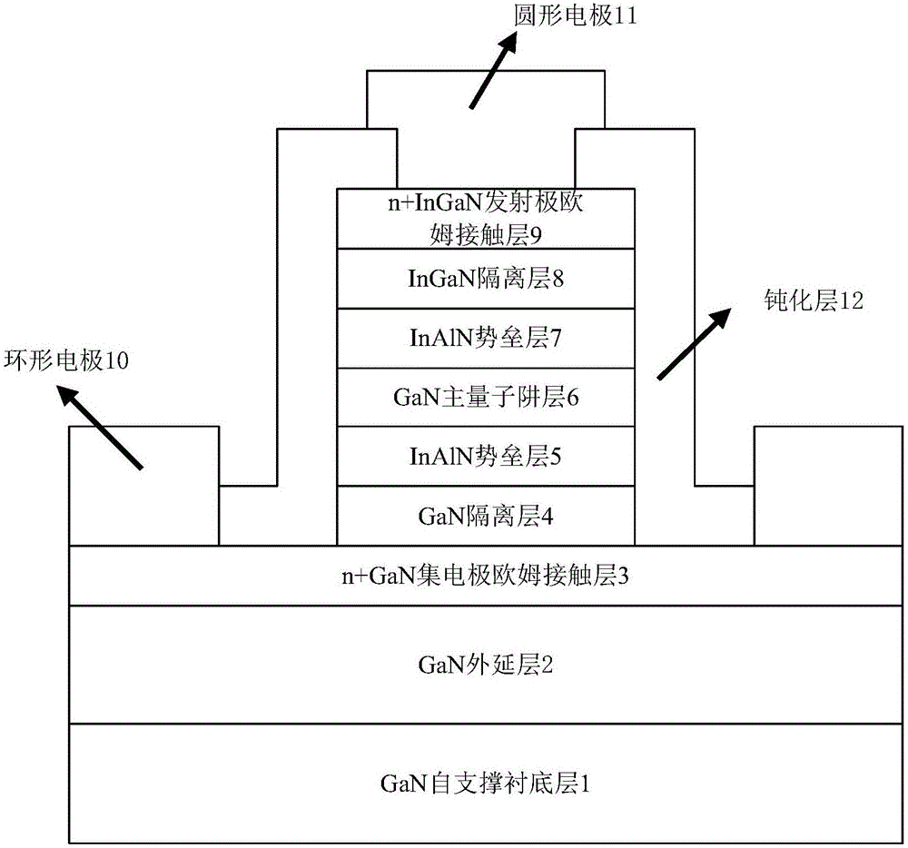
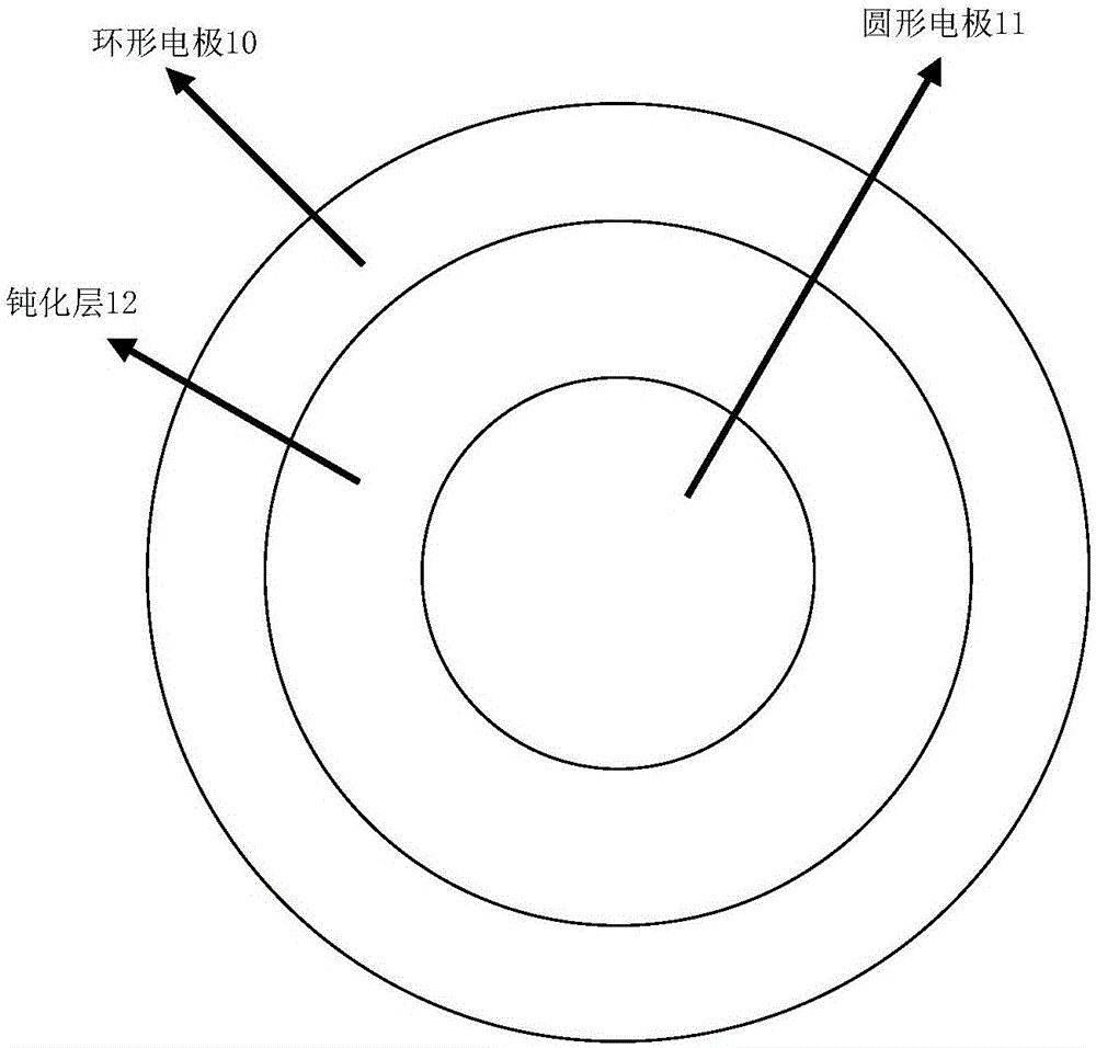
[0113] Example 1: The production thickness is 80nm, the In composition is 3%, and the doping concentration is 1x10 19 n 十 InGaN emitter ohmic contact layer.

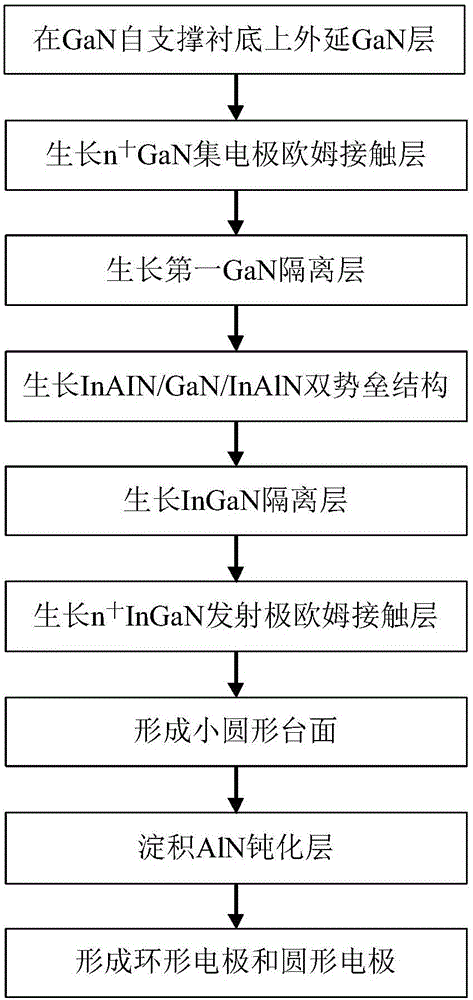
[0114] Step 1: Epitaxial GaN layer on GaN free-standing substrate.

[0115] The GaN epitaxial layer 2 is grown on the substrate 1 by the molecular beam epitaxy MBE method.

[0116] The specific steps of the molecular beam epitaxy MBE method are as follows.

[0117] Prepare sources, using high-purity nitrogen and gallium as nitrogen and gallium sources, respectively.

[0118] Put the substrate 1 into the ultra-high vacuum chamber.

[0119] Raise the gallium furnace to a temperature of 850°C.

[0120] The nitrogen source and the gallium source are sprayed from the jet furnace, the flow rate of nitrogen gas is controlled to be 1.6mL / min, the plasma input power is 400W, and the reflected power is 5W.

[0121] Molecular streams ejected by different sources grow GaN layers on the substrate.

[0122] Step 2: Grow n 十 Ga...

Embodiment 2

[0187] Example 2: The production thickness is 100 nm, the In composition is 5%, and the doping concentration is 5×10 19 n 十 InGaN emitter ohmic contact layer.

[0188] Step A: Epitaxial GaN layer on GaN free-standing substrate.

[0189] The GaN epitaxial layer 2 is grown on the substrate 1 by the molecular beam epitaxy MBE method.

[0190] The specific steps of the molecular beam epitaxy MBE method are as follows.

[0191] Prepare sources, using high-purity nitrogen and gallium as nitrogen and gallium sources, respectively.

[0192] Put the substrate 1 into the ultra-high vacuum chamber.

[0193] Raise the gallium furnace to a temperature of 850°C.

[0194] The nitrogen source and the gallium source are sprayed from the jet furnace, the flow rate of nitrogen gas is controlled to be 1.6mL / min, the plasma input power is 400W, and the reflected power is 5W.

[0195] Molecular streams ejected by different sources grow GaN layers on the substrate.

[0196] Step B: Grow n 十 ...

Embodiment 3

[0261] Example 3: The fabrication thickness is 120 nm, the In composition is 7%, and the doping concentration is 1×10 20 n 十 InGaN emitter ohmic contact layer.

[0262] Step 1: Epitaxial GaN layer on GaN free-standing substrate.

[0263] The GaN epitaxial layer 2 is grown on the substrate 1 by the molecular beam epitaxy MBE method.

[0264] The specific steps of the molecular beam epitaxy MBE method are as follows.

[0265] Prepare sources, using high-purity nitrogen and gallium as nitrogen and gallium sources, respectively.

[0266] Put the substrate 1 into the ultra-high vacuum chamber.

[0267] Raise the gallium furnace to a temperature of 850°C.

[0268] The nitrogen source and the gallium source are sprayed from the jet furnace, the flow rate of nitrogen gas is controlled to be 1.6mL / min, the plasma input power is 400W, and the reflected power is 5W.

[0269] Molecular streams ejected by different sources grow GaN layers on the substrate.

[0270] Step 2: Grow n 十...


PUM

PropertyMeasurementUnit
thicknessaaaaaaaaaa
thicknessaaaaaaaaaa
thicknessaaaaaaaaaa

Abstract

The invention discloses an RTD diode of an indium gallium nitride emitting electrode ohmic contact layer and a manufacturing method thereof. The diode comprises a GaN epitaxial layer, an n+GaN collector electrode ohmic contact layer, a first GaN separating layer, a first InA1N barrier layer, a GaN main quantum well layer, a second InA1N barrier layer, an InGaN separating layer, an n+InGaN emitting electrode ohmic contact layer, a circular electrode, an annular electrode which is arranged above the n+GaN collector electrode ohmic contact layer and is not contacted with the first GaN separating layer and an A1N passivation layer located above the n+GaN collector electrode ohmic contact layer. The emitting electrode ohmic contact layer of the diode adopts an InGaN material so that a peak value current is increased and output power is increased too. In a diode manufacturing method, the InGaN is grown and then a high temperature technology is not needed, In precipitation does not exist and electric leakage of a device is reduced.

Description

technical field [0001] The invention belongs to the technical field of electronics, and further relates to a resonant tunneling diode RTD (Resonant Tunneling Diode) with an ohmic contact layer of an indium gallium nitride InGaN emitter in the technical field of microelectronic devices and a manufacturing method. The invention can be used as a high-frequency and high-power device, and can be applied in the fields of microwave and high-speed digital circuits. Background technique [0002] The resonant tunneling diode RTD of wide-bandgap semiconductor GaN material is a new type of nano-device that works by quantum resonant tunneling effect, and has bistable, self-locking characteristics and obvious negative resistance characteristics. The resonant tunneling diode RTD has a small intrinsic capacitance, so it has a high speed and operating frequency. Compared with other nano-devices, its development is faster and more mature, and it has entered the application stage. With the c...

Claims


Application Information

Patent Timeline
Patent Type & Authority Applications(China)
IPC IPC(8): H01L29/88H01L29/45H01L21/329
CPCH01L29/452H01L29/66219H01L29/882
Inventor 张进成黄金金于婷陆芹郝跃薛军帅杨林安林志宇
Owner XIDIAN UNIV
Why Eureka
Try Eureka