Voltage-mode switching DC-DC converter with on-chip frequency compensation

A DC-DC, voltage mode technology, applied in the direction of output power conversion device, DC power input conversion to DC power output, instruments, etc., can solve the problems of magnification influence, multiplication magnification limited, inconvenient integration, etc., to ensure The effect of improving output voltage accuracy and reducing system offset

Active Publication Date: 2016-10-26
CHENGDU SINO MICROELECTRONICS TECH CO LTD
View PDF4 Cites 10 Cited by
  • Summary
  • Abstract
  • Description
  • Claims
  • Application Information

AI Technical Summary

Problems solved by technology

Since the error amplifier of this control loop works in an internal open-loop state, the loop gain of the system is not fixed, and the inductance L O and output capacitor C O The formed LC filter network will produce double poles, which will cause the phase of the system to change rapidly and produce a ‐180° phase shift. When the system is subject to various interferences such as loop DC gain changes, loop unity gain bandwidth changes, feedback loop oscillations, and noise, etc. Triggered by factors, it is easy to generate loop oscillation
[0004] Therefore, in the design of the switching DC-DC converter, it is necessary to add a compensation network to ensure system stability. The traditional switching DC-DC converter compensation network is composed of passive resistors and capacitors. Since the compensation capacitor is usually relatively large, it is difficult to Integrated, so the compensation network is usually implemented with off-chip discrete devices, which increases the area of ​​the PCB board and the number of pins of the chip, while increasing the application cost, limited to the current trend of miniaturization and low cost of portable products, for switching DC-DC The converter puts forward new requirements, and the external compensation components should be as simple as possible, and can be fully integrated inside the chip to save PCB area and peripheral component costs
[0005] At present, the commonly used internal frequency compensation methods mainly include active capacitance and active resistance schemes based on constant transconductance amplifiers and capacitance multipliers, but the multiplication magnification of active capacitance is limited, the maximum is 100 times, when the compensation capacitance is large , the on-chip capacitance is still very large, which is not easy to integrate. At the same time, the amplification factor is seriously affected by device matching and process parameters. The active resistance is affected by the transconductance of the operational amplifier. The actual resistance is difficult to accurately control, and the design of the active compensation network is difficult. The system is not easy to stabilize

Method used


Image

  • Voltage-mode switching DC-DC converter with on-chip frequency compensation
  • Voltage-mode switching DC-DC converter with on-chip frequency compensation
  • Voltage-mode switching DC-DC converter with on-chip frequency compensation

Examples


Embodiment

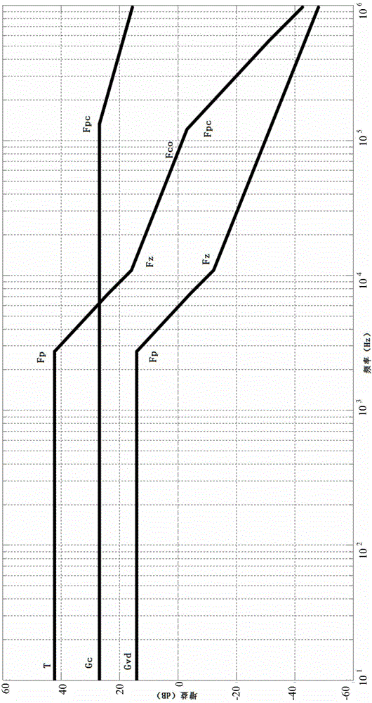
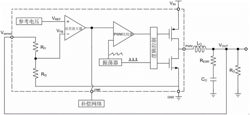
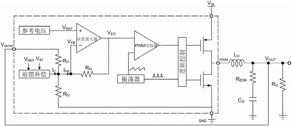
[0048] The specific connection method of the fixed gain error amplifier is as follows Figure 5 shown, the sampling resistor R f1 Connect one end to the output voltage V sense , the other end is connected to the inverting input of the error amplifier V FB , the sampling resistor R f2 One end is connected to the inverting input terminal of the error amplifier V FB , the other end is connected to GND, the feedback resistor R f3 One end is connected to the error amplifier inverting input terminal V FB , the other end is connected to the error amplifier output V EO , due to the feedback resistor R f3 Connected directly between the input and output of the error amplifier, under steady-state conditions, the voltage at the input of the error amplifier, V FB equal to the reference voltage V REF held constant, the error amplifier output voltage V EO Changes with the duty cycle, so the resistance R under different duty cycle conditions f3 The current on I FB Different, the sy...


PUM


Abstract

The invention discloses a voltage-mode switching DC-DC converter with on-chip frequency compensation, and relates to the field of analog integrated circuits. The voltage-mode switching DC-DC converter comprises an error amplifier, a PWM comparator, an oscillator, a logic control module and a power tube, wherein the power tube is provided with a VIN input end used for inputting variable DC voltage VIN. The voltage-mode switching DC-DC converter is characterized by further comprises a feedforward compensation module, wherein an output end of the feedforward compensation module is connected to a negative input end of the error amplifier, the output end of the feedforward compensation module is further grounded through a second resistor Rf2, the output end of the feedforward compensation module is further connected to an output end of the error amplifier through a third resistor Rf3, and the output end of the feedforward compensation module is connected to output voltage Vsense through a first resistor Rf1. The voltage-mode switching DC-DC converter realizes on-chip full integration of compensation components under the condition of ensuring the loop stability, so that the area of a PCB is saved, and the application cost is reduced.

Description

technical field [0001] The invention relates to the field of analog integrated circuits, in particular to a voltage-mode switching DC-DC converter with an on-chip frequency compensation structure. Background technique [0002] The switching DC-DC converter is an important part of the power management circuit, which is used to convert the variable input DC voltage into a fixed output DC voltage. Compared with the LDO voltage regulator, the switching DC-DC converter has high efficiency High advantages, it is one of the preferred power supply systems for portable products. [0003] The structure diagram of the traditional voltage-mode switching DC-DC converter is as follows: figure 1 As shown, it is composed of reference voltage, oscillator, error amplifier, sampling resistor, PWM comparator, logic control, power transistor, external compensation network and LC filter network, and the output voltage is fed back to the error amplifier after being divided by the sampling resisto...

Claims


Application Information

Patent Timeline
Patent Type & Authority Applications(China)
IPC IPC(8): H02M3/156
CPCH02M3/156H02M1/0016
Inventor 冯浪武鹏王洪全李呈
Owner CHENGDU SINO MICROELECTRONICS TECH CO LTD
Why Eureka
Try Eureka