Anisotropic conductive film and method for producing same
An anisotropic, conductive film technology, applied in conductive connection, printed circuit manufacturing, conductive adhesive connection, etc., can solve the problems of IC chips, substrate bending, etc., and achieve the effect of alleviating bending
- Summary
- Abstract
- Description
- Claims
- Application Information
AI Technical Summary
Problems solved by technology
Method used
Image

Examples
preparation example Construction
[0087] >
[0088] Next, an example of the production method of the anisotropic conductive film of the present invention will be described.
[0089] The anisotropic conductive film of the present invention can be produced by performing a low-adhesion region forming process on a part of one surface of the insulating adhesive layer. Examples of the low-adhesive region forming process include pouring a low-adhesive region-forming material and performing smoothing by a known method; raster processing with a laser; or micro-concave-convex processing by photolithography.
[0090] A preferred example of the production method of the anisotropic conductive film of the present invention is a production method having the following steps (A) to (C). Each process is described below.
[0091] Process (A)
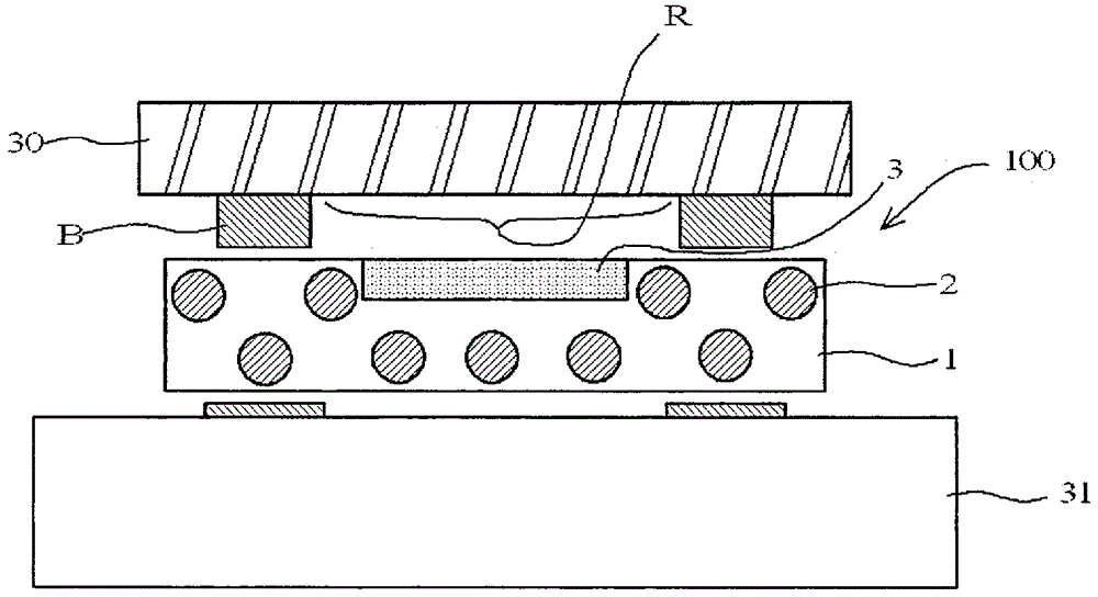
[0092] First, a composition for forming an insulating adhesive layer containing conductive particles is applied on a mold having convex portions corresponding to low-adhesive regions, a...
Embodiment 1~5
[0103] With toluene, 60 parts by mass of phenoxy resin (YP-50, Nippon Steel Sumikin Chemical Co., Ltd.), 40 parts by mass of acrylate (EP600, Daicel-Allnex Ltd. (Daicel-Allnex Ltd. (Daycel Aurnex))), 2 parts by mass of photoradical polymerization initiator (IRGACURE 369, Mitsubishi Chemical Co., Ltd.) and 10 parts by mass of conductive particles (Ni / Au plated resin particles, AUL704, Sekisui Chemical Industry Co., Ltd.) with an average particle diameter of 4 μm ) to prepare a mixed solution so that the resin solid content is 50% by mass.
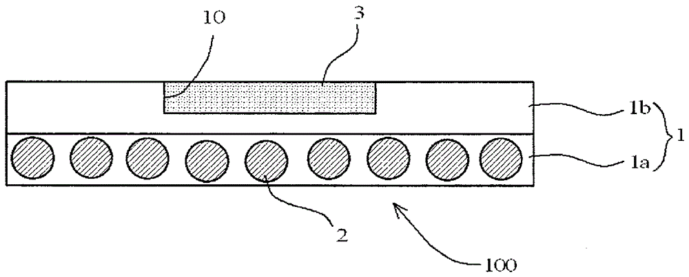
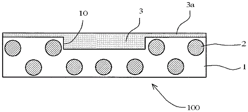
[0104] Using this mixed solution and forming the predetermined protrusions (in the case of Examples 1 to 4, the same Figure 4 The mode of corresponding continuous extending setting, under the situation of embodiment 5 is and Figure 5 Corresponding to the sheet-shaped mold in a discontinuous stepping stone shape), an insulating adhesive layer having a width of 2 mm was prepared after cutting. The insulating adhesive layer was removed from...
Embodiment 6
[0108] (Preparation of Insulating Adhesive Layer Arranged with Conductive Particles)
[0109] With toluene, 60 parts by mass of phenoxy resin (YP-50, Nippon Steel & Sumikin Chemical Co., Ltd.), 40 parts by mass of acrylate (EP600, Daicel-Allnex Ltd. (Daicel-Allnex Ltd. (Daycel Allnex Co., Ltd.)) and 2 parts by mass of a photoradical polymerization initiator (IRGACURE 369, Mitsubishi Chemical Co., Ltd.) prepared a mixed liquid so that the solid content would be 50% by mass. The mixed solution was coated on a polyethylene terephthalate film having a thickness of 50 μm so that the dry thickness would be 8 μm, and dried in an oven at 80° C. for 5 minutes to form a photoradically polymerizable resin layer.
[0110] Next, in the obtained photoradically polymerizable resin layer, conductive particles (Ni / Au plated resin particles, AUL704, Sekisui Chemical Co., Ltd.) having an average particle diameter of 4 μm were arranged in a single layer at a distance of 4 μm. Furthermore, from t...
PUM
| Property | Measurement | Unit |
|---|---|---|
| glass transition temperature | aaaaa | aaaaa |
| thickness | aaaaa | aaaaa |
| thickness | aaaaa | aaaaa |
Abstract
Description
Claims
Application Information