
A preparation method of proximity soft film exposure micro-nano light-trapping structure

A light-trapping structure and proximity technology, applied in the field of solar cells, can solve the problems affecting the accuracy of the imprinting process, the increase in the proportion of hidden cracks in silicon wafers, and the pressure damage of silicon wafers, etc., so as to reduce the accuracy and uniformity , Arrangement controllable, cost reduction effect

Active Publication Date: 2017-06-23
徐州美兴光电科技有限公司
View PDF7 Cites 0 Cited by
  • Summary
  • Abstract
  • Description
  • Claims
  • Application Information

AI Technical Summary

Problems solved by technology

However, in the nanoimprinting disclosed in CN 102148292 B, the pattern template is imprinted into the inside of the mask. After the imprint is exposed, a demoulding process is required. During the demolding process, due to the adhesion between the mask and the pattern template, a part of the mask Adhering to the pattern template, resulting in pattern loss and contamination of the pattern template, which affects the accuracy of the subsequent imprinting process; and the pattern template needs a certain pressure to be imprinted into the mask, which will cause pressure damage to the silicon wafer, resulting in The proportion of cracks in silicon wafers increases, which is not suitable for low-priced thin silicon wafers

Method used


Image

  • A preparation method of proximity soft film exposure micro-nano light-trapping structure
  • A preparation method of proximity soft film exposure micro-nano light-trapping structure
  • A preparation method of proximity soft film exposure micro-nano light-trapping structure

Examples


Embodiment 1

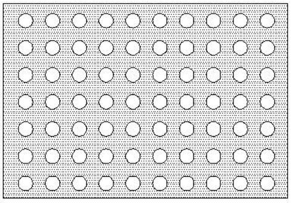
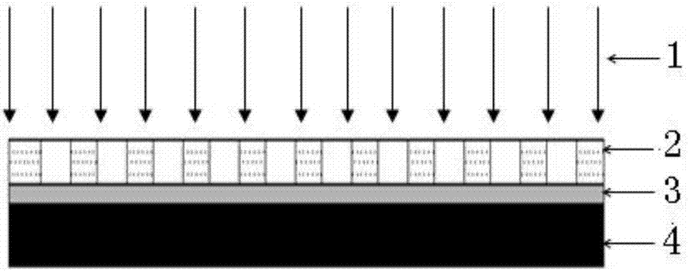
[0045] like figure 1 , figure 2 , image 3 and Figure 4 As shown, a method for preparing a proximity-type soft film exposure micro-nano light trapping structure comprises the following steps:

[0046] 1) Preparation of hard template: The hard template is used as the master of the soft film board, and the material is silicon; the pattern of the hard template is the same as that of the silicon wafer, and the size is 1.2 times that of the silicon wafer. The hard film board is designed by plasma etching technology graphics;

[0047] 2) Convert the hard template graphics to the soft template: the soft template is used as the exposure template, and polydimethylsiloxane (PDMS) is used. The process of making the soft film plate includes:

[0048] (a) firstly, the polydimethylsiloxane is heated to a fluid state, stirred and mixed for 5min;

[0049] (b) cutting the polydimethylsiloxane after stirring on a hard film board placed in the fixture container, the pattern end of the har...

Embodiment 2

[0060] A method for preparing a proximity soft film exposure micro-nano light trapping structure, comprising the following steps:

[0061] 1) Preparation of the hard template: the hard template is the master plate of the soft film board, and the material is gemstone; the pattern of the hard template is the same as that of the silicon wafer, and the size is 1.3 times the size of the silicon wafer. The hard film plate adopts plasma etching technology to obtain the design pattern ;

[0062] 2) Convert the hard template graphics to the soft template, the soft template is used as the exposure template, and the soft template is made of plastic materials, such as polydimethylsiloxane (PDMS) or a mixed material of various components. The process of making the soft film plate includes :

[0063] (a) First heat the plastic material to a fluid state, and stir and mix for 10 minutes;

[0064] (b) Blanking the stirred plastic material on the hard film plate placed in the jig container, t...

Embodiment 3

[0075] A method for preparing a proximity soft film exposure micro-nano light trapping structure, comprising the following steps:

[0076] 1) Preparation of the hard template: the hard template is the master plate of the soft film board, and the material is copper, iron and other metal materials; the pattern of the hard template is the same as that of the silicon wafer, and the size is 1.5 times the size of the silicon wafer. Eclipse technology to get design graphics;

[0077] 2) Convert the hard template graphics to the soft template, the soft template is used as the exposure template, and the soft template is made of plastic materials, such as polydimethylsiloxane (PDMS) or a mixed material of various components. The process of making the soft film plate includes :

[0078] (a) First heat the plastic material to a fluid state, and stir and mix for 20 minutes;

[0079] (b) Blanking the stirred plastic material on the hard film plate placed in the jig container, the pattern ...


PUM


Abstract

The invention discloses a preparation method of a proximity soft membrane exposure micro-nano light trapping structure, and belongs to the technical field of solar cells. The method comprises the following steps of (1) preparing a hard template; (2) transferring a pattern of the hard template to a soft template; (3) pre-cleaning a solar cell silicon wafer and removing a surface damage layer; (4) coating the surface of the cleaned silicon wafer with a photoresist; (5) vertically adsorbing the soft template on the upper surface of the photoresist through vacuum pressure and carrying out exposure in parallel light; (6) pre-drying the exposed silicon wafer, developing the silicon wafer through a developing solution and finally drying the silicon wafer; and (7) obtaining a silicon substrate micro-nano light trapping structure through plasma etching or wet etching. By the micro-nano texture structure prepared by the method, reflection of the silicon substrate surface can be reduced; the texture structure is in a sub-micron scale or a nanoscale, uniform in size and controllable in shape, and is arranged according to a certain mode; and absorption and utilization of sunlight through the solar cell can be improved through the solar cell employing crystal silicon as the substrate.

Description

technical field [0001] The invention relates to a preparation method of a micro-nano texture, in particular to a preparation method of using a proximity soft film to expose a micro-nano light trapping structure on a silicon substrate of a solar cell, and belongs to the technical field of solar cells. Background technique [0002] Conventional fossil fuels are being used up day by day. As a clean energy, solar energy is the most potential energy source to replace fossil fuels. Crystalline silicon solar cell is a semiconductor electronic device that can effectively absorb solar radiation and convert it into electricity. It is currently the mainstream of solar cell development and occupies most of the market share. [0003] In order to reduce the reflectivity of the crystalline silicon surface, in the process of the solar cell, the crystalline silicon surface is textured to increase the absorption of light. Generally, single crystal silicon is etched by alkaline solution, and ...

Claims


Application Information

Patent Timeline
Patent Type & Authority Patents(China)
IPC IPC(8): H01L31/18
CPCH01L31/02363Y02E10/50Y02P70/50
Inventor 涂亮亮刘亚坤林建男魏明德
Owner 徐州美兴光电科技有限公司
Learn More