High brightness AlGaInP light emitting diode with copper substrate and manufacture method thereof

A technology for light-emitting diodes and a manufacturing method, which is applied to electrical components, circuits, semiconductor devices, etc., can solve the problems of reduced light-emitting diode light-emitting efficiency, low current injection efficiency, limited expansion capability, etc., and achieves excellent heat dissipation function, low cost, and increased The effect of light extraction efficiency

Inactive Publication Date: 2016-11-09
YANGZHOU CHANGELIGHT
View PDF4 Cites 5 Cited by
  • Summary
  • Abstract
  • Description
  • Claims
  • Application Information

AI Technical Summary

Problems solved by technology

[0003] Conventional vertical structure AlGaInP light-emitting diodes are based on the P-GaP current spreading layer for lateral expansion, injecting current into the light-emitting area, but due to the limited current spreading ability of P-GaP, the current density in the area near the bottom of the electrode is higher, and the current in the area farther away from the electrode The density is low, resulting in low overall current injection efficiency, which reduces the light extraction efficiency of light-emitting diodes

Method used


Image

  • High brightness AlGaInP light emitting diode with copper substrate and manufacture method thereof
  • High brightness AlGaInP light emitting diode with copper substrate and manufacture method thereof
  • High brightness AlGaInP light emitting diode with copper substrate and manufacture method thereof

Examples


Embodiment Construction

[0028] One, concrete implementation steps of the present invention:

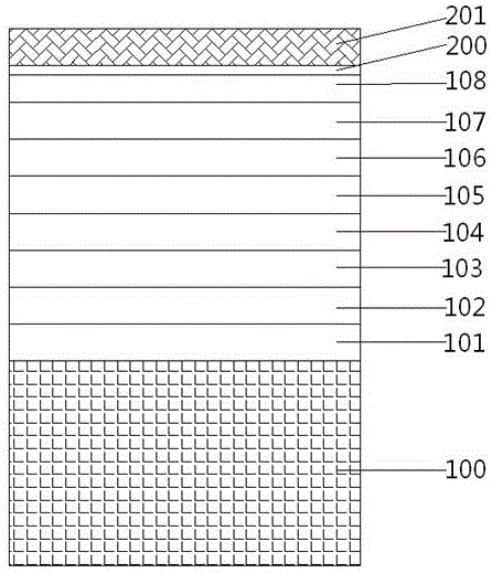
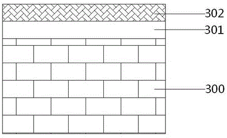
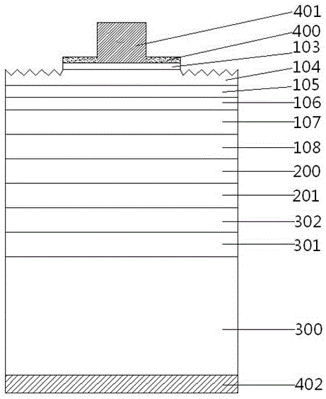
[0029] 1. On the GaAs temporary substrate 100 as the epitaxial layer, the n-GaAs buffer layer 101, the GaInP barrier layer 102, the n-GaAs ohmic contact layer 103, and the roughened n- AlGaInP layer 104, n-AlGaInP confinement layer 105, MQW active layer 106, p-AlGaInP confinement layer 107, p-GaP current spreading layer 108.

[0030] Wherein the GaAs temporary substrate 100 has a thickness of 250-350 μm.

[0031] The n-GaAs ohmic contact layer 103 has a thickness of 30-500nm, preferably 45nm, and a silicon doping concentration of 1×10 18 cm -3 ~3×10 18 cm -3 (in this example, preferably 1×10 18 cm -3 above).

[0032] The thickness of the roughenable n-AlGaInP layer 104 is 0.5-3 μm.

[0033] The thickness of the P-GaP current spreading layer 108 is 2-5 μm, and the magnesium doping concentration is 8×10 17 cm -3 ~1×10 19 cm -3 .

[0034] Clean the p-GaP current spreading layer 108 with 511 soluti...


PUM

PropertyMeasurementUnit
thicknessaaaaaaaaaa
thicknessaaaaaaaaaa
porosityaaaaaaaaaa

Abstract

The invention relates to a high brightness AlGaInP light emitting diode with a copper substrate and a manufacture method thereof, and belongs to the technical field of LED production and application. The copper substrate with the thickness of 150-200 mum is taken as a permanent substrate, and a bonding layer is made at one side. An epitaxial process is performed at one side of a temporary substrate, and an epitaxial wafer is formed. A chip is made by bonding the copper substrate and the epitaxial wafer through the bonding layer. The manufacture method is characterized in that when an n-GaAs ohmic contact layer is manufactured, silicon is doped, and when a p-GaP current extension layer is manufactured, magnesium is doped; after the p-GaP current extension layer is manufactured, an indium tin oxide transparent conducting layer is manufactured on the p-GaP current extension layer, and then a gold reflector layer is vapor-plated on the indium tin oxide transparent conducting layer. According to the invention, the photoelectric effect is increased, and the luminous intensity of the light emitting diode is greatly improved.

Description

technical field [0001] The invention belongs to the technical field of LED production and application, in particular to the chip manufacturing technology of AlGaInP light-emitting diodes. Background technique [0002] Quaternary LED chips are widely used in indicating and displaying various devices due to their high luminous efficiency, wide color range, low power consumption, long life, monochromatic light emission, fast response, impact resistance, and small size. , automotive interior indicator lights, home appliance indicator lights, traffic stop lights, and household lighting, especially the demand for high-brightness and high-power light-emitting diode components has greatly increased. Therefore, the research and production of high-brightness light-emitting diodes must be stepped up. To meet the needs of high-brightness light-emitting diodes in the lighting market. [0003] Conventional vertical structure AlGaInP light-emitting diodes are based on the P-GaP current sp...

Claims


Application Information

Patent Timeline
Patent Type & Authority Applications(China)
IPC IPC(8): H01L33/00H01L33/64
CPCH01L33/0066H01L33/0093H01L33/641
Inventor 肖和平王宇孙如剑郭冠军李威张英马祥柱杨凯
Owner YANGZHOU CHANGELIGHT
Why Eureka
Try Eureka