Receptor-modified and receptor-free titanium dioxide nano metal film Raman chips and manufacturing method

A nano-metal film and titanium dioxide technology, applied in Raman scattering, material excitation analysis, etc., can solve the problems of large absolute quantitative analysis error, poor consistency and stability, and harsh requirements for the production of silver particle film.

Active Publication Date: 2016-11-23
大连世佩达光谱智能检测科技有限公司
View PDF5 Cites 2 Cited by
  • Summary
  • Abstract
  • Description
  • Claims
  • Application Information

AI Technical Summary

Problems solved by technology

[0009] At present, almost all high-sensitivity SERS Raman active substrates have the problems of poor repeatability, consistency and stability of the analysis results, and the error is too large for absolute quantitative analysis. The problem of no results; the fundamental reason is that the production of the silver particle film requires very fine and harsh requirements - the size of the silver particle is required to be resonantly coupled with the wavelength of the exciting laser beam, and the silver particles must be close together, with a distance of ≤2nm, which is difficult to obtain. It is even more difficult to do it, and it is even more difficult to require each silver particle film product to meet the same standard; if the average spacing of silver particles is greater than 4 nanometers, the Raman signal of SERSp will be an order of magnitude lower; therefore, in the SERS silver particle film If there are no strict control methods and control standards in the manufacturing process, it will not be possible to solve the problems of poor repeatability, consistency and stability of SERSp analysis results

Method used


Image

  • Receptor-modified and receptor-free titanium dioxide nano metal film Raman chips and manufacturing method
  • Receptor-modified and receptor-free titanium dioxide nano metal film Raman chips and manufacturing method
  • Receptor-modified and receptor-free titanium dioxide nano metal film Raman chips and manufacturing method

Examples


Embodiment Construction

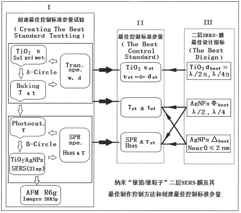
[0027] 1. The specific implementation method of the capillary-type titanium dioxide nano-metal film Raman chip with or without acceptors

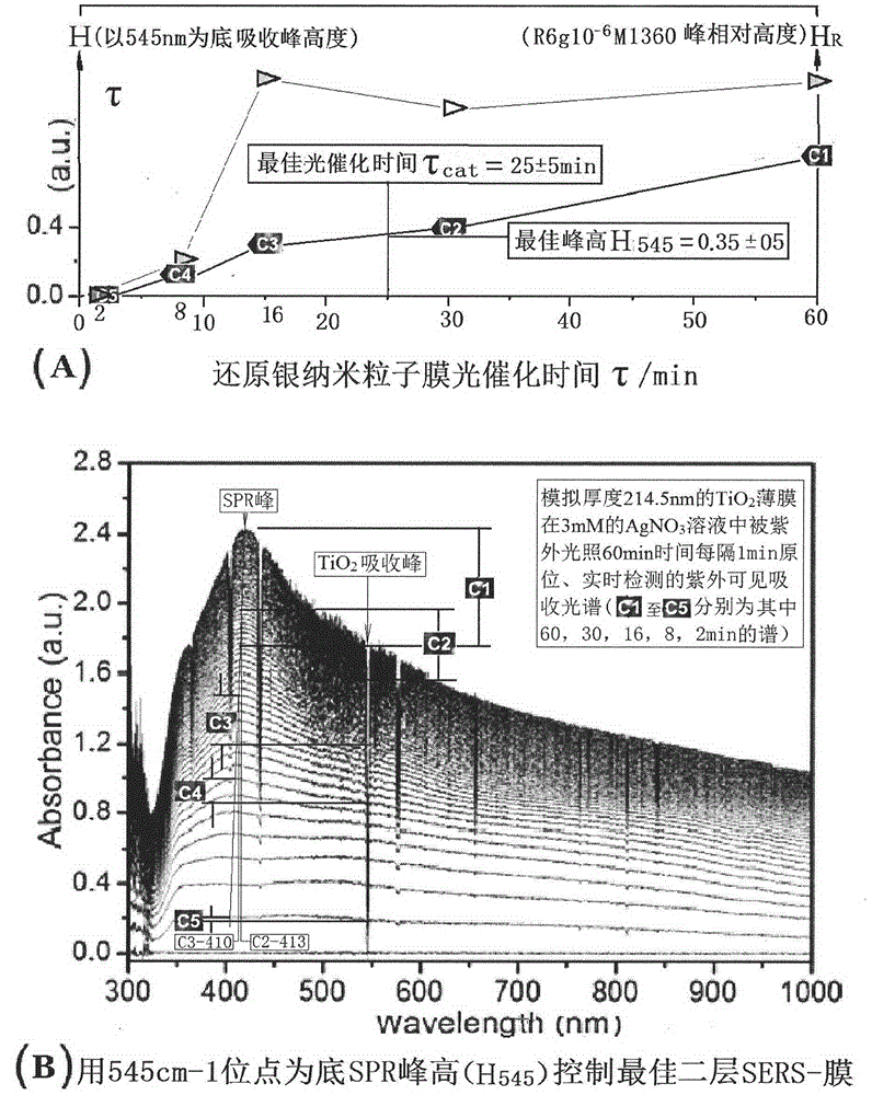
[0028] For the structure of the capillary Raman chip see Figure 6 , coated with TiO in the capillary (1) 2 Membrane (2), TiO 2 Nano "silver foil / silver particles" film (3) is grown on the film, and the acceptor molecular film (4) is modified on the film, and there are very fine engravings near both ends of the capillary inlet and outlet sealing sections (5). Before using the chip, it can be conveniently broken, opened, and spared at the mark at this moment; the specific implementation method of the capillary Raman chip is as follows:

[0029]Step 1: Clean the hard neutral glass or quartz glass capillary, with an inner diameter of about 0.5mm, an outer diameter of 1.0mm, and a length of 100mm;

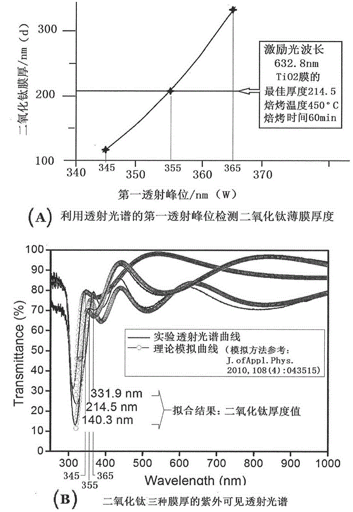
[0030] Step 2: Preparation of TiO 2 Sol: 50mL of butyl titanate and 3mL of acetylacetone were mixed and stirred for 10min (referred to as solut...


PUM


Abstract

The invention discloses receptor-modified and receptor-free titanium dioxide nano metal film Raman chips and a manufacturing method. Each chip is composed of a surface enhanced Raman scattering (SERS) film and a carrier thereof, the carriers comprise the capillary type carrier, the small box type carrier and the microfluidic channel type carrier, the SERS-films comprise the receptor-modified SERS-film and the receptor-free SERS-film, and six types of the Raman chips are obtained. Control standards are set in the manufacturing method, and the controllable SERS-film manufacturing method comprises the steps that 1, a titanium dioxide film is pulled through a sol-gel method, and scattered particles are crystallized; 2, a second-layer nano silver foil/silver particle SERS-film grows through photocatalysis; 3, the second-layer SERS-film is modified with specifically coordinated and combined receptor molecules through hydrogen bonding force or immune bonding force according to the needs of detected object donor molecules, and then a third-layer SERS-film is formed. The Raman chips can be applied to environmental pollution treatment and detection, hard drug and warfare agent detection, pesticide residue detection, harmful food additive screening, large-scale early-stage cancer Raman screening and the like.

Description

technical field [0001] The invention relates to the field of Raman analysis chips in spectral analysis technology, in particular to a Raman chip with or without acceptor titanium dioxide nanometer metal film and a manufacturing method. Background technique [0002] The surface near-field enhanced Raman spectroscopy (SERSp) analysis technology established by the principle of the surface near-field enhanced Raman scattering (SERS) effect is the most commonly used method of mixing nano-silver particles and liquid phase samples into the capillary. Raman sample cell; In addition, a variety of Raman sample cell technical solutions have been disclosed, for example: first build TiO on the inner wall of the capillary 2 Nanotube arrays, silver nanoparticles modified on TiO by Sn ion coupling 2 Capillary sample cell on the surface of the tube array "CN102706857A, a method for preparing a multifunctional surface-enhanced Raman scattering substrate"; three-dimensional porous and ordered...

Claims


Application Information

Patent Timeline
Patent Type & Authority Applications(China)
IPC IPC(8): G01N21/65
Inventor 吴世法
Owner 大连世佩达光谱智能检测科技有限公司
Why Eureka
Try Eureka