Two-way ultralow capacitance transient voltage suppressor and production method thereof

A technology of transient voltage suppression and capacitance, which is applied in the direction of electric solid-state devices, semiconductor/solid-state device manufacturing, circuits, etc., can solve the problems of increasing diebonding costs, increasing packaging defects, increasing overall size, etc., achieving low packaging costs and meeting The effect of application requirements

Active Publication Date: 2016-11-23
BEIJING YANDONG MICROELECTRONICS
View PDF6 Cites 5 Cited by
  • Summary
  • Abstract
  • Description
  • Claims
  • Application Information

AI Technical Summary

Problems solved by technology

[0009]1. Two sets of chips need to be packaged in series, which is expensive;
[0010]2. For smaller packages, two sets of chips cannot be packaged at the same time
[0013]1. The two channel terminals must be led out from the front side at the same time, resulting in a larger chip area, which is not suitable for smaller packages;
[0014]2. When packaging, the two channel ends must each have a metal wire, whic

Method used


Image

  • Two-way ultralow capacitance transient voltage suppressor and production method thereof
  • Two-way ultralow capacitance transient voltage suppressor and production method thereof
  • Two-way ultralow capacitance transient voltage suppressor and production method thereof

Examples


Embodiment Construction

[0089] In order to illustrate the present invention more clearly, the present invention will be further described in detail below in conjunction with preferred embodiments and accompanying drawings. The same parts in the drawings are denoted by the same symbols. Those skilled in the art should understand that the content specifically described below is illustrative rather than restrictive, and should not limit the protection scope of the present invention.

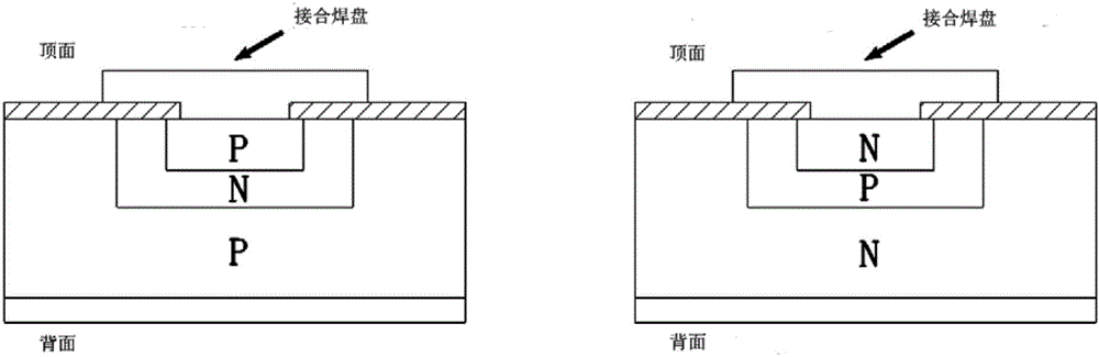
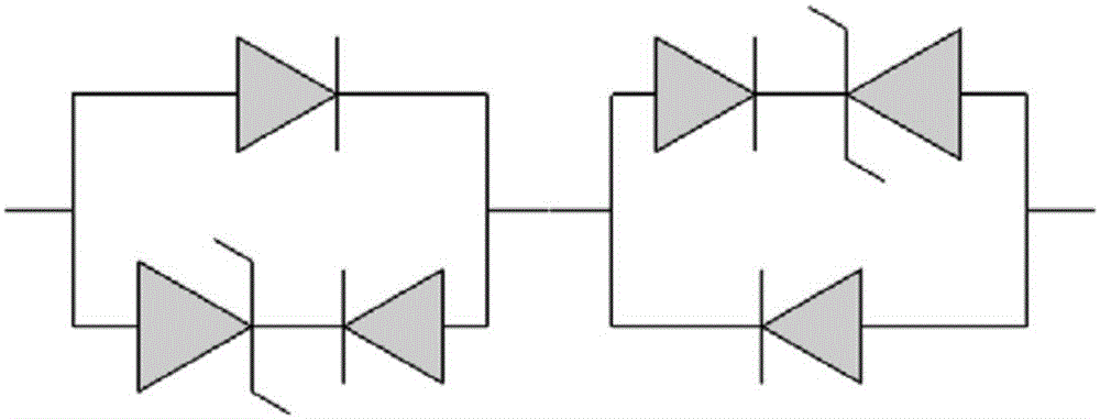
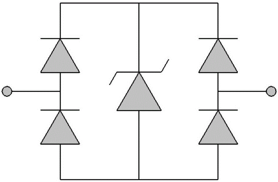
[0090] Such as Figure 5 As shown, the bidirectional ultra-low capacitance TVS of the present invention includes a first TVS transistor 15 , a second TVS transistor 16 , an upper rectifier diode 17 and a lower rectifier diode 18 . Wherein, the cathode of the first TVS tube 15 is connected with the cathode of the upper rectifying diode 17, the lower rectifying diode 18 shares the anode with the first TVS tube 15 and the second TVS16 tube, and the anode of the upper rectifying diode 17 is connected with the cathode of the l...


PUM

PropertyMeasurementUnit
Resistivityaaaaaaaaaa
Thicknessaaaaaaaaaa
Resistivityaaaaaaaaaa

Abstract

The invention relates to a two-way ultralow capacitance TVS (Transient Voltage Suppressor) and a production method thereof. The TVS comprises a semiconductor substrate of a first conductive type, a first epitaxial layer of a second conductive type, a third epitaxial layer of the first conductive type, a first buried layer of the second conductive type, a first doped region of the second conductive type, a second doped region of the first conductive type, a first groove, a second groove, a first insulating medium, a third groove and an active region, wherein the first buried layer is formed between the first epitaxial layer and the third epitaxial layer; the first doped region is formed by being opposite to the first buried layer in the third epitaxial layer; the second doped region is formed in the third epitaxial layer and is not opposite to the first buried layer; the first groove extends to the inside of the semiconductor substrate from the surface of the third epitaxial layer; the second groove extends from the surface of the third epitaxial layer and penetrates through the third epitaxial layer; the first groove and the second groove are filled with the first insulating medium; the third groove extends from the surface of the third epitaxial layer and penetrates through the first buried layer to the inside of the first epitaxial layer; the active region is formed by annealing in-situ polycrystalline silicon loaded in the third groove.

Description

technical field [0001] The invention relates to the technical field of semiconductor microelectronics, in particular, the invention relates to a bidirectional ultra-low capacitance transient voltage suppressor and a manufacturing method thereof. Background technique [0002] Transient Voltage Suppressor TVS (Transient Voltage Suppressor) is a high-efficiency circuit protection device developed on the basis of voltage regulator tubes. The shape of TVS diodes is the same as that of ordinary Zener tubes. However, due to the special structure and process design, the transient response speed and surge absorption capacity of TVS diodes are much higher than ordinary Zener tubes. For example, TVS diodes have a response time of only 10 -12 seconds, and can absorb surge power up to several thousand watts. Under reverse application conditions, when subjected to a high-energy large pulse, the working impedance of the TVS diode will quickly drop to an extremely low conduction value, al...

Claims


Application Information

Patent Timeline
IPC IPC(8): H01L27/02H01L27/08H01L21/822
CPCH01L27/0255H01L27/0296H01L27/0814H01L21/822
Inventor 周源淮永进徐远
Owner BEIJING YANDONG MICROELECTRONICS
Why Eureka
Try Eureka