Manufacturing method of self-alignment low-voltage super-junction MOFET

A manufacturing method and self-alignment technology, applied in the fields of semiconductor/solid-state device manufacturing, electrical components, circuits, etc., can solve problems such as abnormal device parameters and device failure, and achieve the goal of increasing the number of devices, reducing device production costs, and optimizing parameters. Effect

Active Publication Date: 2016-12-07
XIAN LONTEN RENEWABLE ENERGY TECH
View PDF2 Cites 9 Cited by
  • Summary
  • Abstract
  • Description
  • Claims
  • Application Information

AI Technical Summary

Problems solved by technology

[0004] At present, in the production and manufacture of large-sized low-voltage super-junction MOSFETs, the source area is large, and there is no problem with hole alignment. However, with the development of s

Method used


Image

  • Manufacturing method of self-alignment low-voltage super-junction MOFET
  • Manufacturing method of self-alignment low-voltage super-junction MOFET
  • Manufacturing method of self-alignment low-voltage super-junction MOFET

Examples


Embodiment 1

[0064] An embodiment of the present invention provides a method for manufacturing a low-voltage super-junction MOSFET. The method is as follows: filling polysilicon through deep grooves, two deep grooves are mutually charge-balanced to complete the super-junction function, and then wet etching is used to form a shallow MOSFET above the deep grooves. Grooves, low-voltage super-junction MOSFETs are fabricated in shallow trenches to form low-voltage super-junction devices.

[0065] An embodiment of the present invention provides a method for manufacturing a low-voltage super-junction MOSFET, which is implemented through the following steps:

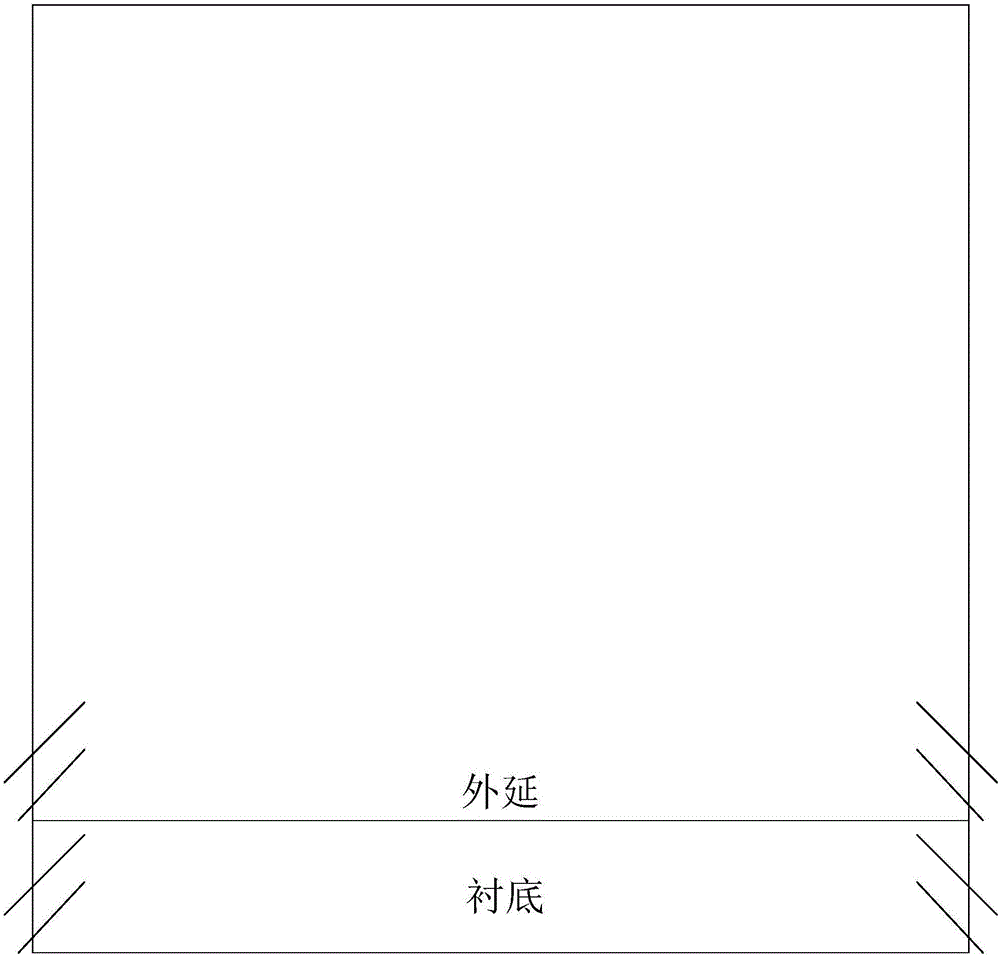
[0066] Step 1: Provide an n-type heavily doped n+ substrate, and form an n-type epitaxial layer on the n+ substrate, such as figure 1 Show;

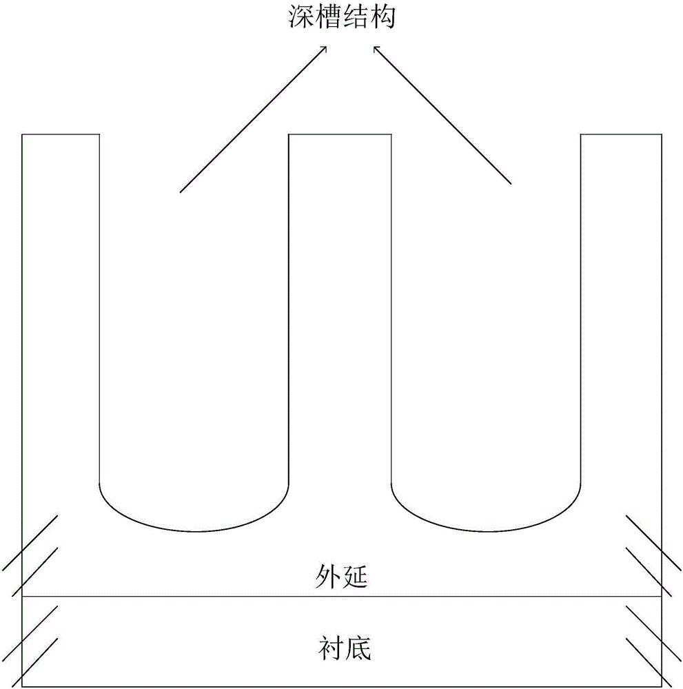
[0067] Step 2: On the n-type epitaxy, form multiple array-type strip-shaped deep grooves by photolithography and dry etching, such as figure 2 Show;

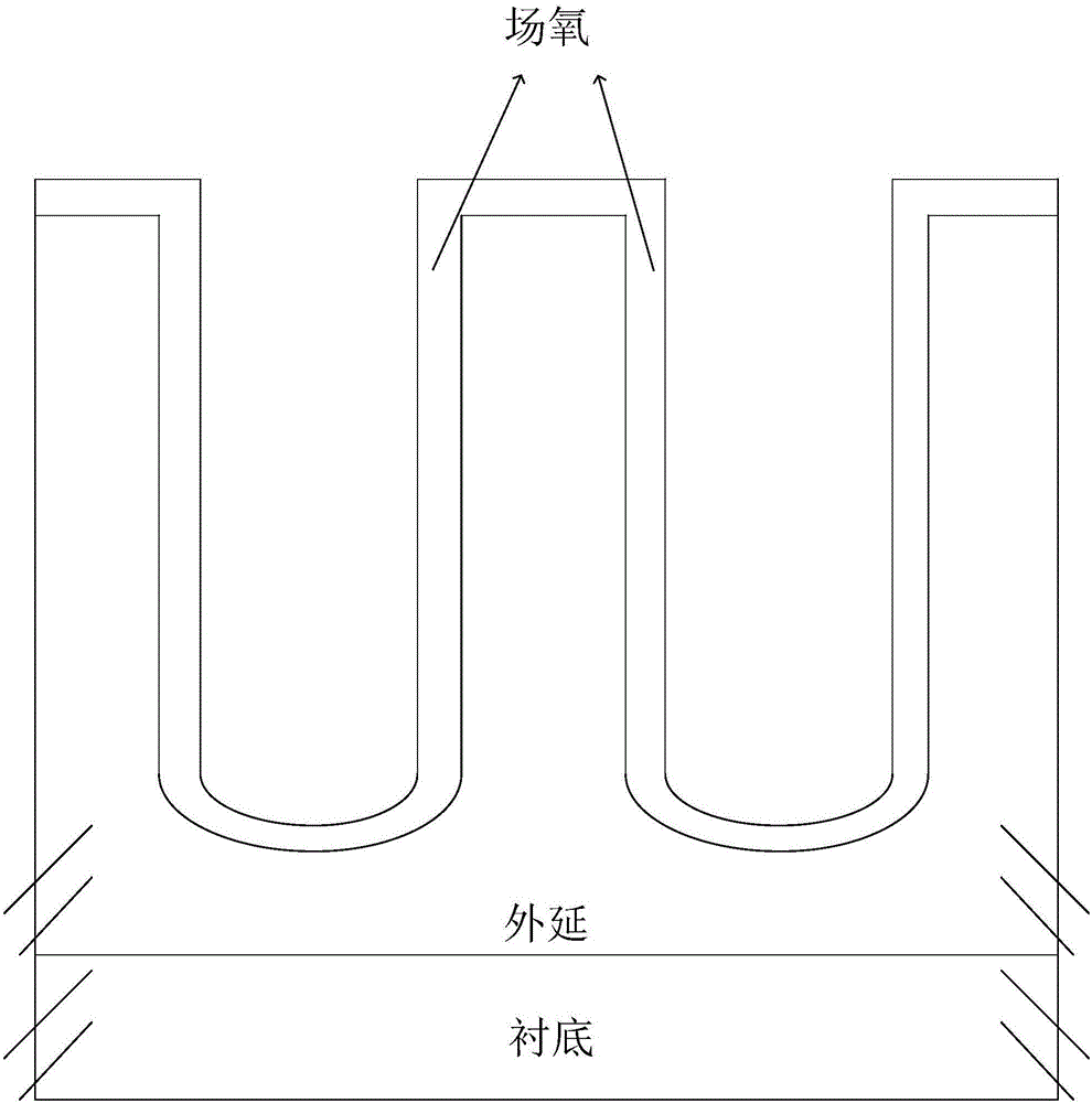
[0068] Step 3: using a thermal oxidation process...

Embodiment 2

[0087] The embodiment of the present invention also provides a method for manufacturing a self-aligned low-voltage super-junction MOSFET, which is characterized in that the method is implemented through the following steps:

[0088] Step 1: providing an n-type heavily doped n+ substrate, and forming an n-type epitaxial layer on the n+ substrate;

[0089] Step 2: Forming deep trenches in the active region and deep trenches in the terminal region by photolithography and dry etching on the n-type epitaxy, and the deep trenches in the terminal region surround the deep trenches in the active region;

[0090] Step 3: using a wet thermal oxidation process to grow a field oxide layer on the bottom and sidewalls of the deep trench;

[0091] Step 4: using the polysilicon deposition process to perform the first polysilicon deposition;

[0092] Step 5: Etching back the polysilicon through a dry etching process until the polysilicon is flush with the upper surface of the epitaxial layer; ...


PUM


Abstract

The invention discloses a manufacturing method of a self-alignment low-voltage super-junction MOFET. A terminal region deep trench formed on n-type epitaxy surrounds an active area deep trench; field oxides grow on the bottom sand the side walls of the deep trenches; primary polycrystalline silicon deposition is carried out; etching is carried out till polycrystalline silicon is flush with the upper surface of an epitaxial layer; secondary polycrystalline silicon deposition is carried out; secondary polycrystalline silicon dry method back etching is carried out to form a shallow slot MOSFET device grid; a P trap is formed; a high-thickness oxidation layer is formed, and the oxidation layer is removed; a device active area is manufactured; contact hole etching is carried out, a light resistor of the whole active area of a small cell area is switched on, a light resistor of a terminal hole demand area is switched on, and small cell area self-alignment hole etching is carried out; ohmic contact is formed through contact hole etching injection, and finally the structure is completed. On the premise of keeping the process cost unchanged, the area of a source area and a single cell can be reduced, and the whole chip area can be reduced.

Description

technical field [0001] The invention belongs to the technical field of semiconductor power devices, and in particular relates to a method for manufacturing a self-aligned low-voltage super-junction MOSFET. Background technique [0002] For traditional power MOSFET devices, there is a certain trade-off relationship between device on-resistance (Ron) and source-drain breakdown voltage (Ron∝BV 2.5 ), has limited the development of power MOSFET devices for a long time. The low-voltage super-junction MOSFET uses the principle of charge balance, so that the N-type drift region can achieve a higher breakdown voltage of the device even under the condition of a higher doping concentration, thereby obtaining a low on-resistance, breaking the traditional silicon power MOSFET. limit. However, due to the development of small-scale devices, the small-scale is becoming more and more stringent for the photolithographic alignment process. [0003] In addition to the good electrical perfor...

Claims


Application Information

Patent Timeline
IPC IPC(8): H01L21/336
CPCH01L29/66477
Inventor 杨乐刘挺岳玲
Owner XIAN LONTEN RENEWABLE ENERGY TECH
Why Eureka
Try Eureka