Nonvolatile memory

A non-volatile, memory technology, applied in electric solid state devices, semiconductor devices, electrical components, etc., can solve the problems of affecting the electrical performance of memory cells, reducing the reliability of memory components, and depleting the tunnel oxide layer. speed, lowering the erase voltage, lowering the effect of the operating voltage

Active Publication Date: 2016-12-07
IOTMEMORY TECH +1
View PDF7 Cites 9 Cited by
  • Summary
  • Abstract
  • Description
  • Claims
  • Application Information

AI Technical Summary

Problems solved by technology

However, the shortening of the gate length will shorten the channel length (Channel Length) under the tunnel oxide layer, which will easily cause abnormal electrical penetration (Punch Through) between the drain and the source, which will seriously affect the memory cell. electrical performance
Moreover, when programming and / or erasing memory cells, electrons repeatedly pass through the tunnel oxide layer, which will wear out the tunnel oxide layer, resulting in reduced reliability of the memory element.

Method used


Image

  • Nonvolatile memory
  • Nonvolatile memory
  • Nonvolatile memory

Examples


Embodiment Construction

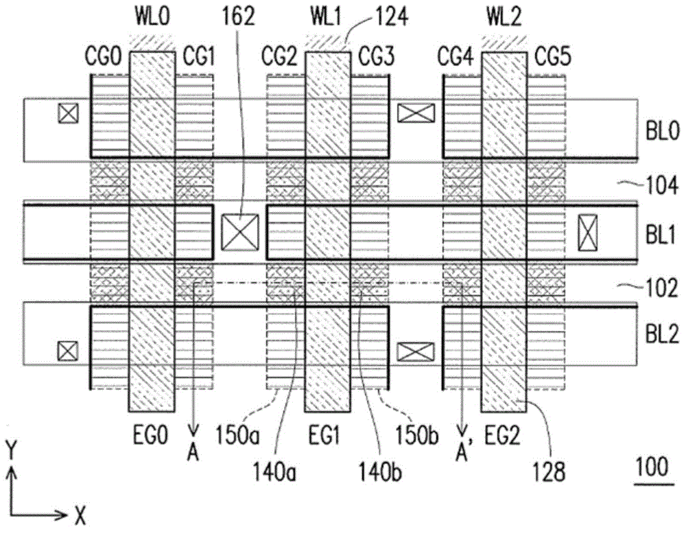
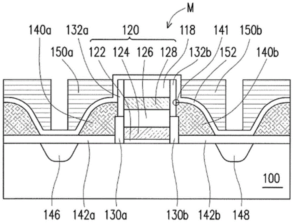
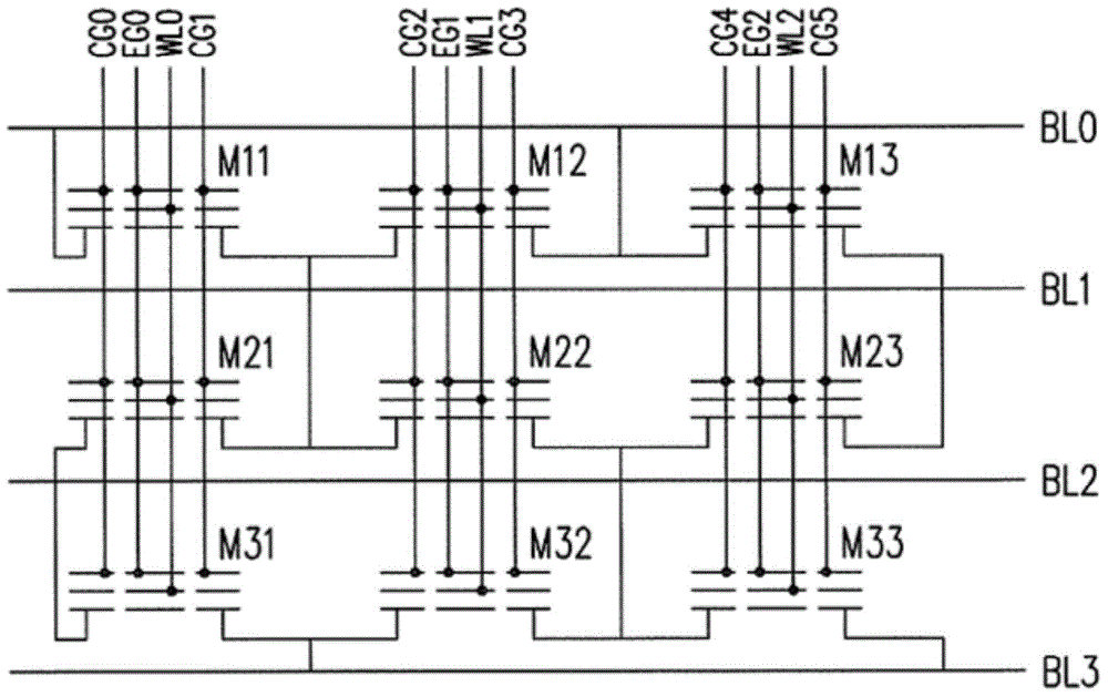
[0068] Figure 1A It is a top view of a non-volatile memory shown in an embodiment of the present invention. Figure 1B It is a schematic cross-sectional view of a non-volatile memory shown in an embodiment of the present invention. Figure 1B shown as along the Figure 1A Sectional view of line A-A' in the middle. Figure 1C It is a schematic circuit diagram of a non-volatile memory shown in an embodiment of the present invention.

[0069] Please refer to Figure 1A , Figure 1B and Figure 1C , the nonvolatile memory includes a plurality of memory cells M11-M33, word lines WL0-WL2, erase lines EG0-EG2, bit lines BL0-BL3, and control gate lines CG0-CG5. The memory cells M11-M33 are arranged in a row / column array.

[0070] A nonvolatile memory is provided on the substrate 100 . For example, an isolation structure 102 is disposed in the substrate 100 to define an active region 104 . The isolation structure 102 is, for example, a shallow trench isolation structure.

[007...


PUM


Abstract

The invention provides a nonvolatile memory. The nonvolatile memory is provided with a storage unit, wherein the storage unit is provided with a stack structure, a first floating gate, a second floating gate, erase gate dielectric layers, auxiliary gate dielectric layers, a first doping region, a second doping region, a first control gate and a second gate, wherein the stack structure comprises a gate dielectric layer, an auxiliary gate, an insulation layer and an erase gate which are sequentially arranged, the first floating gate and the second floating gate are respectively arranged on side walls of two sides of the stack structure, the erase gate dielectric layers are arranged between the erase gate and the first floating grid and between the erase gate and the second floating grid, the auxiliary gate dielectric layers are arranged between the auxiliary gate and the first floating gate and between the auxiliary gate and the second floating gate, the first doping region and the second doping region are respectively arranged at two sides of the stack structure, the first floating gate and the second floating gate, and the first control gate and the second gate are respectively arranged on the first floating gate and the second floating gate. By the nonvolatile memory, low-voltage operation can be performed, and the reliability of a semiconductor component is further improved.

Description

technical field [0001] The invention relates to a semiconductor element, in particular to a nonvolatile memory. Background technique [0002] Non-volatile memory has been widely used in personal computers and electronic devices due to its advantages that data can be stored, read, and erased multiple times, and the stored data will not disappear after power failure. [0003] A typical non-volatile memory is designed to have a stacked gate (Stack-Gate) structure, which includes a tunnel oxide layer, a floating gate (Floating gate), and an inter-gate dielectric that are sequentially arranged on the substrate. layer and control gate (Control Gate). When programming or erasing the flash memory device, appropriate voltages are applied to the source region, the drain region, and the control gate, so that electrons are injected into the polysilicon floating gate, or electrons are removed from the polysilicon floating gate. Set the gate to pull out. [0004] In the operation of th...

Claims


Application Information

Patent Timeline
Patent Type & Authority Applications(China)
IPC IPC(8): H01L27/115
Inventor 郑育明
Owner IOTMEMORY TECH
Why Eureka
Try Eureka