Flexile and large-area perovskite solar cell module and preparation method thereof
A technology of solar cell components and perovskites, which is applied in the manufacture of electrical components, electrical solid devices, semiconductor/solid devices, etc., can solve the problems of difficult industrialization of solar cells, high cost of large-area components, and fracture of ITO conductive layer and other problems, to achieve low-temperature cross-linking curing, high yield, and low equipment requirements
- Summary
- Abstract
- Description
- Claims
- Application Information
AI Technical Summary
Problems solved by technology
Method used
Image
Examples
Embodiment 1
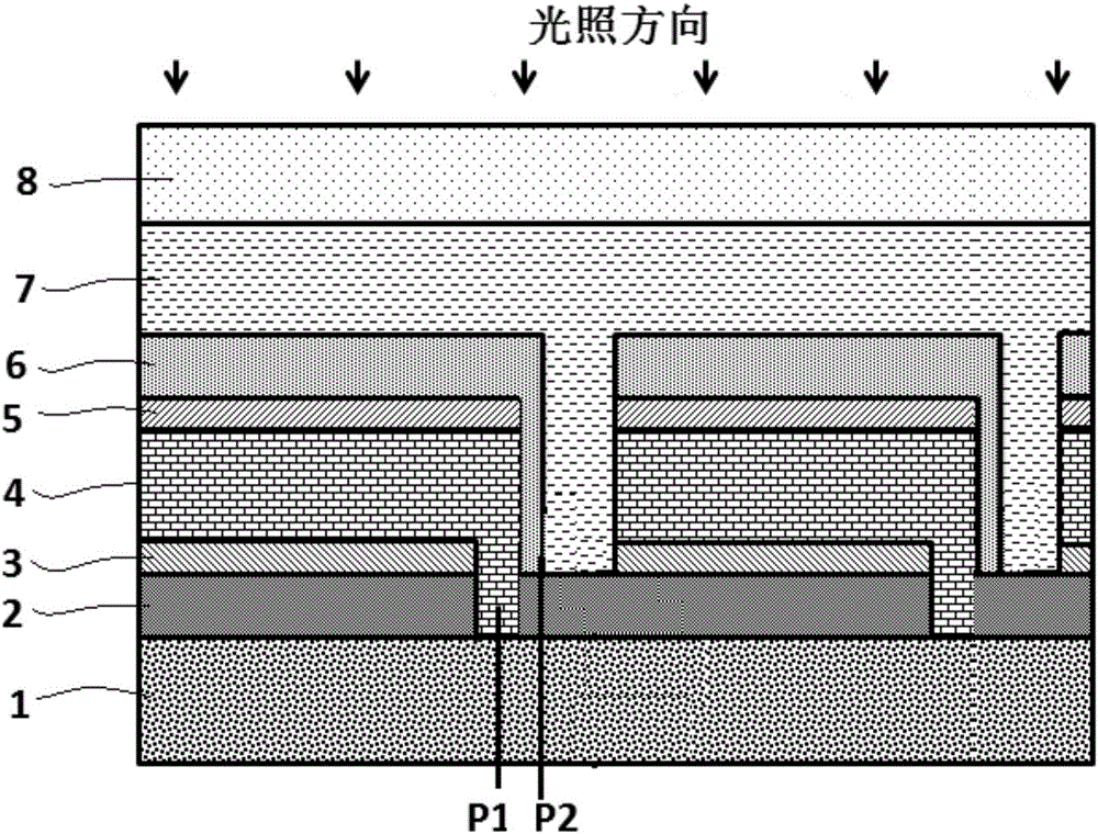
[0034] see figure 1 As shown, a flexible large-area perovskite solar cell module includes a metal back reflection layer Ag, an electron transport layer doped with aluminum-doped zinc oxide (AZO), calcium Titanium absorbing layer CH 3 NH 3 PB 3 , a hole transport layer CuI, a transparent conductive front electrode ITO, a transparent encapsulant, a flexible transparent plastic cover, and light is incident from the direction of the flexible transparent plastic cover.
[0035] Through the two-step scribing process, the large-area module is divided into sub-cells. The metal back reflective layer Ag of the adjacent sub-cell is separated by the P1 scribe groove, and the transparent conductive front electrode ITO of the previous sub-cell is connected to the metal back reflector Ag of the next sub-cell through the P2 scribe groove, so that each sub-cell to form a series structure.
Embodiment 2
[0037] A method for preparing a flexible large-area perovskite solar cell assembly, comprising the steps of:
[0038] Polyimide (PI) flexible plastic substrate cleaning.
[0039] A metal back reflection layer Ag is deposited on the substrate by pulsed DC magnetron sputtering: the substrate temperature is 25-100°C, the sputtering pressure is 0.1-10Pa, the sputtering power is 50-300W, and the Ag film thickness is 50-300nm.
[0040] The electron transport layer AZO is deposited on the Ag film by radio frequency magnetron sputtering: the deposition temperature is 25-100°C, the sputtering pressure is 0.1-10Pa, the sputtering power is 50-300W, and the AZO film thickness is 30-100nm;
[0041] A P1 scribed groove is prepared by laser scribing method with a width of 50-300 μm. The P1 scribe cuts off the AZO and Ag electrodes, touching the PI substrate.
[0042] Deposition of CH on the electron transport layer by two-step sequential low-vacuum deposition3 NH 3 PB 3 Absorber layer: P...
PUM
| Property | Measurement | Unit |
|---|---|---|
| Width | aaaaa | aaaaa |
Abstract
Description
Claims
Application Information
