Heterojunction cell with thermal oxidation improved passivation layer interface and preparation method of heterojunction cell
A technology of thermal oxide layer and heterojunction, which is applied in the field of solar cells, can solve the problems of low conversion efficiency of solar cells and reduced minority carrier life, and achieve the effect of improving surface defect structure, increasing minority carrier life, and reducing recombination centers
- Summary
- Abstract
- Description
- Claims
- Application Information
AI Technical Summary
Problems solved by technology
Method used
Image
Examples
Embodiment 1
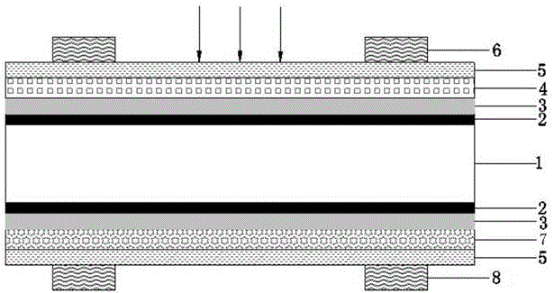
[0023] like figure 1 As shown, an N-type crystalline silicon substrate is taken as an example for illustration. The thermal oxidation of the present invention improves the cross-section of the passivation layer heterojunction solar cell, including: N-type crystalline silicon substrate 1, N-type crystalline silicon substrate 1 The thickness is 50-200um, and the resistivity is ~5Ω·cm; it has a front side and a back side, and is sequentially arranged on the front side of the N-type crystalline silicon substrate 1: thermal oxide layer 2, intrinsic amorphous silicon thin film layer 3, N Type doped layer, that is, the front doped layer 4, the transparent conductive film layer 5 and the front metal gate line 6; on the back of the N-type crystalline silicon substrate 1 are arranged in sequence: thermal oxide layer 2, intrinsic amorphous silicon film layer 3 , P-type doped layer, that is, the back doped layer 7 , the transparent conductive film layer 5 and the back metal grid line 8 . ...
Embodiment 2
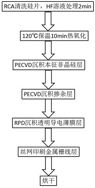
[0025] like figure 1 , 2 As shown, taking an N-type crystalline silicon substrate as an example for illustration, the method for preparing a heterojunction solar cell with improved passivation layer cross-section by thermal oxidation of the present invention includes the following steps:
[0026] S1: surface treatment: perform standard RCA cleaning on the N-type crystalline silicon substrate 1, and treat it with HF solution for 2 minutes before performing PECVD;
[0027] S2: Prepare a thermal oxide layer: put the substrate treated in step S1 into a holding furnace, and hold it at 120°C under normal pressure for 10 minutes in an air atmosphere, and grow a 1-5nm oxide layer on the front and back of the substrate respectively;
[0028] S3: Preparing a doped layer: depositing an N-type doped layer and a P-type doped layer on the intrinsic amorphous silicon film layer on the front and back of the N-type crystalline silicon substrate 1, respectively;
[0029] S4: Prepare a transpa...
PUM
| Property | Measurement | Unit |
|---|---|---|
| Thickness | aaaaa | aaaaa |
| Resistivity | aaaaa | aaaaa |
Abstract
Description
Claims
Application Information

