A kind of interconnection solder and its interconnection forming method

A technology of solder and phase composition, applied in the field of materials, can solve the problem of long time consumption of transient liquid phase method, and achieve the effects of long time consumption, high melting point and good electrical conductivity.

Active Publication Date: 2018-10-26
HARBIN INST OF TECH SHENZHEN GRADUATE SCHOOL
View PDF10 Cites 0 Cited by
  • Summary
  • Abstract
  • Description
  • Claims
  • Application Information

AI Technical Summary

Problems solved by technology

[0008] In view of the above technical problems, the present invention discloses an interconnection solder and its interconnection forming method. The joint formed by the interconnection solder realizes the controllability of Young's modulus and thermal expansion coefficient in the atmospheric environment, and provides an interconnection solder Continuous forming method, which assists rapid prototyping, the invention not only solves the problem of long time-consuming transient liquid phase method, but also can adjust the Young's modulus of the joint to avoid thermal stress failure caused by chip heat generation

Method used


Image

  • A kind of interconnection solder and its interconnection forming method
  • A kind of interconnection solder and its interconnection forming method
  • A kind of interconnection solder and its interconnection forming method

Examples


Embodiment 1

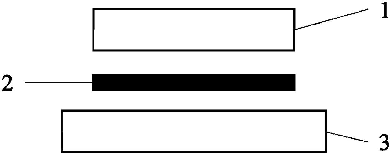
[0053] see figure 1 , figure 2 and Figure 4 As shown, a method for realizing a high melting point compound joint under an atmospheric environment, the connection method includes the following steps:

[0054] Ⅰ. Surface treatment of the materials to be connected: Use 1200# sandpaper to slightly polish the connection surface of the base material 1 and base material 3 3 to remove the oxide layer and oily impurities on the surface, and then immerse in absolute ethanol solution for ultrasonic cleaning 3 ~5min;

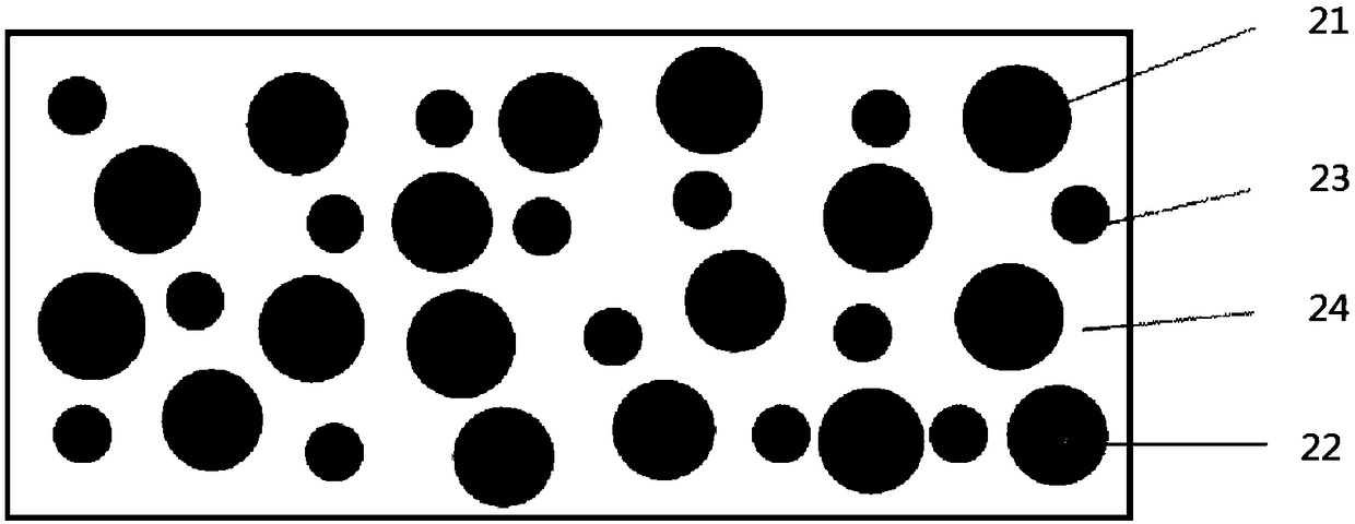
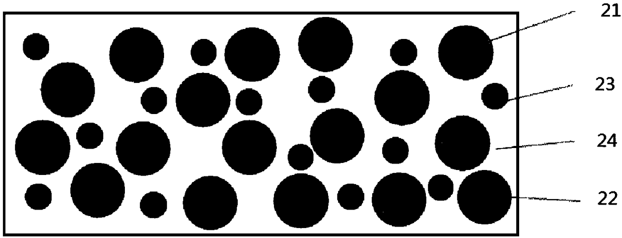
[0055] Ⅱ. Place the base material 33 on the lower layer, the base material 1 on the upper layer and the middle layer 22 in the middle to form a sandwich structure, the base material 1 and the base material 3 3 are placed horizontally and laterally. The base material 1 used above is a chip, the chip material is Si, SiC, GaN, InP or GaAs, the coating metal on the back of the chip is Ni, and the thickness of the Ni layer is 8 μm; the base material 3 3 is a pure Ni substra...

Embodiment 2

[0063] See attached figure 1 , figure 2 and Figure 4 As shown, a method for quickly realizing a hybrid joint connection between a high melting point compound and a high melting point metal in an atmospheric environment, the connection method includes the following steps:

[0064] Ⅰ. Surface treatment of the materials to be connected: Use 1200# sandpaper to polish the surface of the connection surface of the base material 1 and base material 3 3 to remove oil and impurities on the surface, and then immerse in absolute ethanol solution for ultrasonic cleaning for 3-5 minutes.

[0065] Ⅱ. Place the base material 33 on the lower layer, the base material 1 on the upper layer and the middle layer 22 in the middle to form a sandwich structure, the base material 1 and the base material 3 3 are placed horizontally and laterally. The base material 1 used above is a chip, the chip material is Si, SiC, GaN, InP or GaAs, the coating metal on the back of the chip is Ni, and the thickness ...

Embodiment 3

[0072] see figure 1 and Figure 4 As shown, a method for quickly realizing the connection of high-melting point compounds, high-melting point metals and third-phase metal mixed tissue joints in an atmospheric environment, the connection method includes the following steps:

[0073] Ⅰ. Surface treatment of the materials to be connected: Use 1200# sandpaper to polish the surface of the connection surface of the base material 1 and base material 3 3 to remove oil and impurities on the surface, and then immerse in absolute ethanol solution for ultrasonic cleaning for 3-5 minutes.

[0074] Ⅱ. Place the base material 33 on the lower layer, the base material 1 on the upper layer and the middle layer 22 in the middle to form a sandwich structure, the base material 1 and the base material 3 3 are placed horizontally and laterally. The base material 1 used above is a chip, the chip material is Si, SiC, GaN, InP or GaAs, the coating metal on the back of the chip is Ni, and the thickness...


PUM

PropertyMeasurementUnit
melting pointaaaaaaaaaa
thicknessaaaaaaaaaa

Abstract

The invention provides an interconnection brazing material and an interconnection forming method thereof. The heating technological temperature of a product applied by the interconnection brazing material is T, the interconnection brazing material contains a component A with the melting point larger than T, a component B with the melting point smaller than T and a third-phase component C with the melting point larger than T; the third-phase component C accounts 0-30% the total mass of the component A, the component B and the third-phase component C. A compound AxBy is formed through a reaction between the component A and the component B at the heating technological temperature; the ratio of amounts of substances of the component A to the component B is larger than x / y, the third-phase component C does not react with the component A or the component B, the hardness of the third-phase component C is smaller than those of the component A, the component B and the compound AxBy. According to the technical scheme, a high-melting-point welding joint is obtained, and the Young modulus and the thermal expansion coefficient of a joint can be adjusted by adjusting the proportion of the components inside the brazing material.

Description

technical field [0001] The invention belongs to the technical field of materials, and in particular relates to an interconnect solder and an interconnect forming method thereof. Background technique [0002] In recent years, wide and tight band semiconductors such as SiC, GaN, and InP have replaced Si with their superior electronic conversion performance and are widely used in automotive electronics, high-power LEDs, and other fields. These electronic devices can work in an environment higher than 250°C and maintain excellent characteristics. On the other hand, microelectronic chip bonding is developing rapidly in the direction of miniaturization, high density, and excellent electromechanical properties, which greatly increases the heat generated per unit area. Due to the limitation of the thermal conductivity of the material itself, the heat cannot be dissipated from the outside world in time. The exchange causes the operating temperature of the chip to become higher and h...

Claims


Application Information

Patent Timeline
Patent Type & Authority Patents(China)
IPC IPC(8): B23K35/22B23K1/06B23K35/26
CPCB23K1/06B23K35/22B23K35/262B23K2101/36
Inventor 计红军李明刚
Owner HARBIN INST OF TECH SHENZHEN GRADUATE SCHOOL
Why Eureka
Try Eureka