A mems package with heat sink and magnetic shield and preparation method thereof

A magnetic shielding and heating technology, which is applied in semiconductor/solid-state device manufacturing, electrical components, electric solid-state devices, etc., can solve problems such as external electromagnetic signal interference, weak signal interference, MEMS sensors can not work normally, etc., to achieve material realization, Effects of shortening the hot start time and shortening the thermal equilibrium time

Active Publication Date: 2018-05-29
INST OF GEOLOGY & GEOPHYSICS CHINESE ACAD OF SCI
View PDF3 Cites 0 Cited by
  • Summary
  • Abstract
  • Description
  • Claims
  • Application Information

AI Technical Summary

Problems solved by technology

However, the electromagnetic signals or magnetic signals flooded in the external environment will cause huge interference to the weak signals detected by the MEMS sensor, making the MEMS sensor unable to work normally. For example, for the most common MEMS capacitive sensors (MEMS accelerometers, gyroscopes, etc. Many sensors are based on this principle), and the capacitance change detected by it is in the order of pF / fF or even aF. Such a small capacitance change is easily disturbed by external electromagnetic signals. If you want to get the correct detection result, you need Interference signals must be shielded

Method used


Image

  • A mems package with heat sink and magnetic shield and preparation method thereof
  • A mems package with heat sink and magnetic shield and preparation method thereof
  • A mems package with heat sink and magnetic shield and preparation method thereof

Examples


Embodiment 1

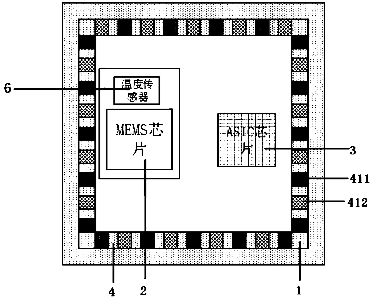
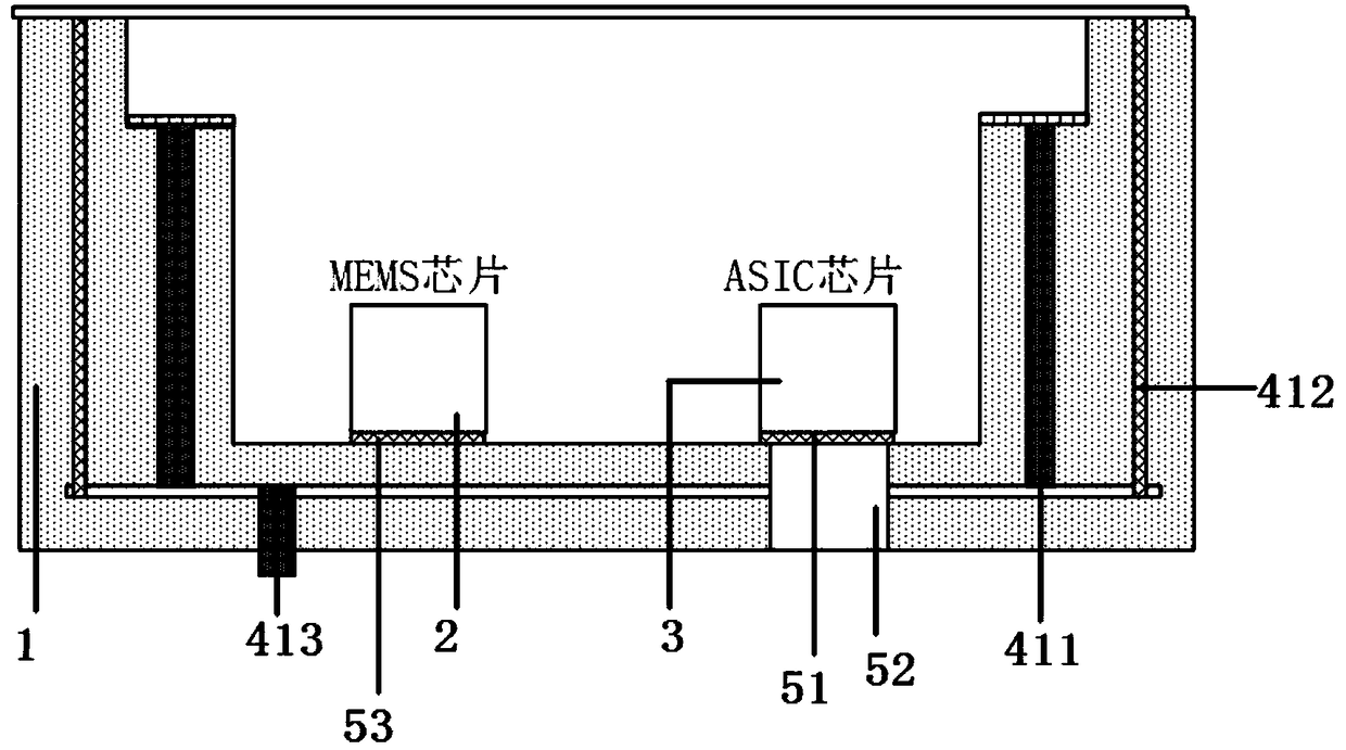
[0054] Such as figure 1 with image 3 As shown, a MEMS package with a heat sink and magnetic shielding, the MEMS package includes a package shell 1, a MEMS chip 2, an ASIC chip 3 and a temperature sensor 6, the package shell 1 is a cuboid structure, including four The side wall, the packaging tube shell is provided with a magnetic shielding passage, the magnetic shielding passage includes a metal vertical passage 41, a metal cover plate 42 and a metal bottom plate 43, the metal bottom plate 43 is a metal plate or a metal mesh, and the metal vertical The passage 41 includes a plurality of metal strips, and the plurality of metal strips are built in parallel on the side wall of the package package 1 in the vertical direction, and the plurality of metal strips include signal metal strips 411 and magnetic shielding metal strips 412. The signal metal strip 411 and the magnetic shielding metal strip 412 are arranged on the same layer, the signal metal strip 411 is used for signal t...

Embodiment 2

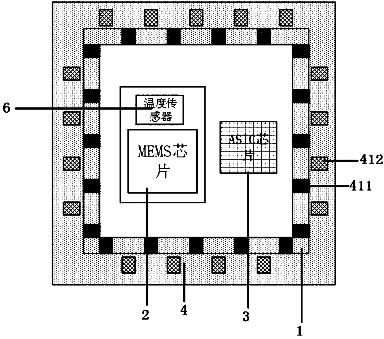
[0059] Such as Figure 2-Figure 3 As shown, a MEMS package with a heat sink and magnetic shielding, the MEMS package includes a package shell 1, a MEMS chip 2, an ASIC chip 3 and a temperature sensor 6, the package shell 1 is a cuboid structure, including four The side wall, the packaging tube shell is provided with a magnetic shielding passage, the magnetic shielding passage includes a metal vertical passage 41, a metal cover plate 42 and a metal bottom plate 43, the metal bottom plate 43 is a metal plate or a metal mesh, and the metal vertical The passage 41 includes a plurality of metal strips, and the plurality of metal strips are built in parallel on the side wall of the package package 1 in the vertical direction, and the plurality of metal strips include signal metal strips 411 and magnetic shielding metal strips 412. The signal metal strip 411 and the magnetic shielding metal strip 412 are arranged on different layers, the signal metal strip 411 is located near the inn...


PUM


Abstract

The invention provides a MEMS packaging structure with heat sink and electromagnetic shielding and a preparation method thereof. The MEMS packaging structure comprises a package shell, a MEMS chip and an ASIC chip, wherein the package shell is provided with an electromagnetic shielding path and a fast heat conduction channel. Dense metallic vertical paths are disposed on the sidewalls of the package shell to shield electromagnetic influence from a side and can be connected with the MEMS chip or the ASIC chip to output MEMS and ASIC signals. A metal cover plate and a metal base plate performs electromagnetic shielding from the top and the bottom of the package shell respectively at the same time, and achieve the electromagnetic shielding of the entire packaging structure in cooperation with the metallic vertical paths; The ASIC is connected to a thermal conduction column through glue with good thermal conductivity to achieve heat sink and reduce the impact of heat. The glue under the MEMS chip is high in thickness and small in size and a part of the MEMS chip is suspended so as to achieve effective thermal insulation.

Description

technical field [0001] The invention belongs to the field of micro-electromechanical systems, and in particular relates to a MEMS package with a heat sink and a magnetic shield and a preparation method thereof. Background technique [0002] Microelectromechanical Systems (MEMS for short) is an industrial technology that integrates microelectronics technology and mechanical engineering, and its operating range is in the micron range. A smaller, similar technology in the nanometer range is known as nanoelectromechanical systems (US term). As a product of the integration of microelectronics and micromechanics, micromechanical electronic systems combine silicon microfabrication technology in integrated circuit manufacturing technology and micromachining technology in the machinery industry to create machines, electronics, and even optical, The new device that integrates machine and electricity has broad application prospects. For example, some new cars are equipped with a varie...

Claims


Application Information

Patent Timeline
Patent Type & Authority Patents(China)
IPC IPC(8): H01L23/367H01L23/552H01L21/56
Inventor 薛旭张潇筱辛维郭士超
Owner INST OF GEOLOGY & GEOPHYSICS CHINESE ACAD OF SCI
Why Eureka
Try Eureka