Double-gate MOSFET structure and preparation method thereof

A technology of gate metal layer and gate dielectric layer, which is applied in semiconductor/solid-state device manufacturing, semiconductor devices, electrical components, etc., can solve the problems of limiting the radio frequency performance of double-gate devices and large parasitic capacitance, and reduce the short channel effect , reduced parasitic capacitance, and high channel carrier mobility

Active Publication Date: 2017-01-04
INST OF MICROELECTRONICS CHINESE ACAD OF SCI
View PDF5 Cites 3 Cited by
  • Summary
  • Abstract
  • Description
  • Claims
  • Application Information

AI Technical Summary

Problems solved by technology

However, due to the relatively large contact area between the back gate and the channel and the source and drain of the traditional double-gate structure MOSFET, the parasitic capacitance is relatively large, which limits the radio frequency performance of the double-gate device. Reduced contact area between source and drain

Method used


Image

  • Double-gate MOSFET structure and preparation method thereof
  • Double-gate MOSFET structure and preparation method thereof
  • Double-gate MOSFET structure and preparation method thereof

Examples


Embodiment Construction

[0049] In order to make the object, technical solution and advantages of the present invention clearer, the present invention will be further described in detail below in conjunction with specific embodiments and with reference to the accompanying drawings.

[0050] This embodiment specifically describes a double-gate MOSFET structure and its preparation method provided by the present invention.

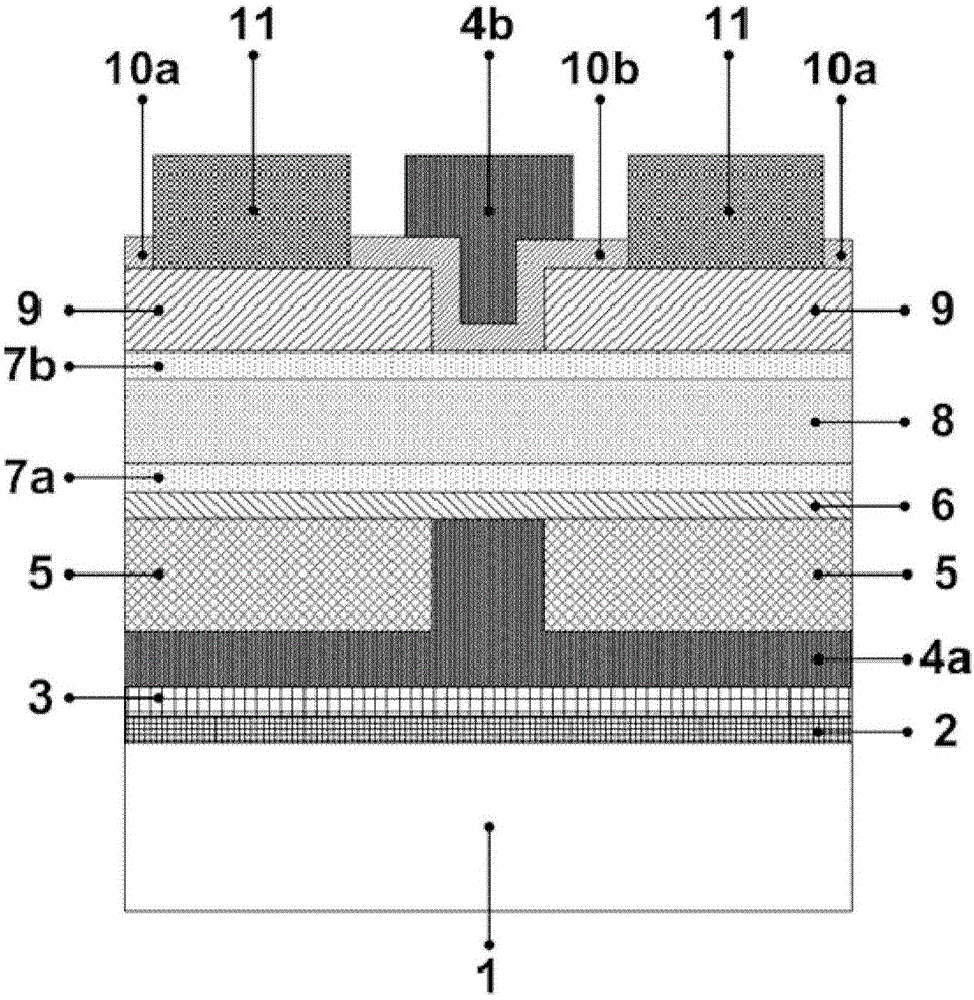
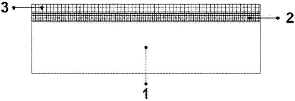
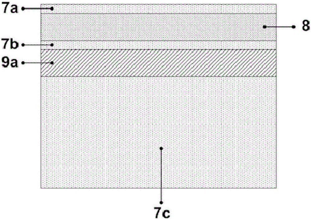
[0051] Such as figure 1 As shown, the double-gate MOSFET structure provided by the present invention includes a single crystal silicon substrate 1, an isolation layer 2, a bonding metal layer 3, a first gate metal layer 4a, a deparasitic dielectric layer 5, First gate dielectric layer 6, first interface control layer 7a, III-V group semiconductor channel layer 8, second interface control layer 7b, second gate dielectric layer 10b, third gate dielectric layer 10a, second gate metal layer 4b, III-V semiconductor source-drain layer 9, source-drain metal layer 11;

[0052] The isolatio...


PUM

PropertyMeasurementUnit
thicknessaaaaaaaaaa
thicknessaaaaaaaaaa
thicknessaaaaaaaaaa

Abstract

The invention discloses a double-gate MOSFET structure and a preparation method thereof, and belongs to the technical field of semiconductor integration. The double-gate MOSFET structure sequentially comprises a first gate metal layer, an III-V group semiconductor channel layer, an III-V group semiconductor source drain layer and a second gate metal layer from bottom to top, wherein the first gate metal layer and the second gate metal layer form the double-gate structure; the III-V group semiconductor channel layer and the III-V group semiconductor source drain layer are made of an III-V group semiconductor material. Due to adoption of the double-gate structure, the gate control property of an MOSFET device can be effectively improved, and influence caused by short channel effects and the like can be reduced. As a back gate structure is achieved by using a through hole technique, parasitic capacitance can be effectively reduced, and the radio properties of a device are improved. The double-gate MOSFET structure disclosed by the invention is integrated on a silicon substrate, and single chip integration with other silicon-based CMOS integrated device can be achieved.

Description

technical field [0001] The invention relates to the technical field of semiconductor integration, in particular to a double-gate MOSFET structure and a preparation method thereof. Background technique [0002] As the core and foundation of the information industry, semiconductor technology is regarded as an important symbol to measure a country's scientific and technological progress and comprehensive national strength. In the past 40 years, the integrated circuit technology based on silicon CMOS technology has followed Moore's law to increase the working speed of the chip, increase the integration level and reduce the cost by reducing the feature size of the device. The feature size of the integrated circuit is reduced from the micron scale. to the nanoscale. However, when the gate length of MOS devices is reduced to the 90nm technology node, traditional silicon-based CMOS devices are facing more and more problems. The introduction of new structures and new materials has b...

Claims


Application Information

Patent Timeline
Patent Type & Authority Applications(China)
IPC IPC(8): H01L29/20H01L29/423H01L29/78H01L21/336
CPCH01L29/20H01L29/42356H01L29/66484H01L29/7831
Inventor 孙兵刘洪刚王盛凯常虎东龚著靖
Owner INST OF MICROELECTRONICS CHINESE ACAD OF SCI
Why Eureka
Try Eureka