High-speed groove MOS device and preparing method thereof

A technology of MOS devices and trenches, which is applied in the manufacture of semiconductor/solid-state devices, electric solid-state devices, semiconductor devices, etc., can solve the problems of occupying chip area and cost, occupying silicon surface area, and large overall area, so as to reduce manufacturing costs , high product performance, simple production process

Active Publication Date: 2017-01-11
华羿微电子股份有限公司
View PDF6 Cites 6 Cited by
  • Summary
  • Abstract
  • Description
  • Claims
  • Application Information

AI Technical Summary

Problems solved by technology

The disadvantage is still high cost, high requirements for packaging, and large overall area after packaging
[0007] The third stage is to design and manufacture trench MOSFETs and Schottky diodes in the same chip. The method of processing trench MOSFETs and Schottky diodes is to use partition design and differentiated manufacturing schemes, and realize through wire bonding. Interconnection still occupies a large amount of chip area and cost
Therefore, the disadvantages are always: 1. The Schottky diode structure occupies a large amount of silicon surface area, resulting in large chip area and high cost; 2. The process is complicated, resulting in high manufacturing cost.

Method used


Image

  • High-speed groove MOS device and preparing method thereof
  • High-speed groove MOS device and preparing method thereof
  • High-speed groove MOS device and preparing method thereof

Examples


Embodiment Construction

[0067] The present invention will be further described in detail below in conjunction with the accompanying drawings, so that those skilled in the art can implement it with reference to the description.

[0068] It should be understood that terms such as "having", "comprising" and "including" used herein do not exclude the presence or addition of one or more other elements or combinations thereof.

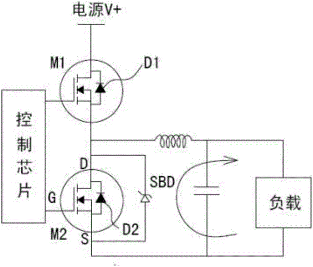
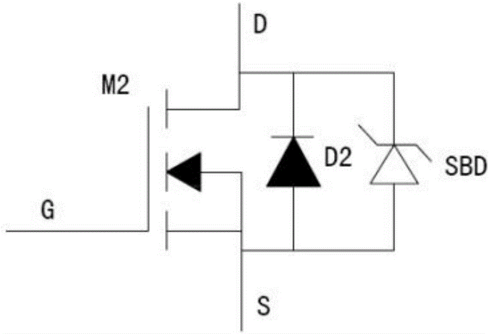
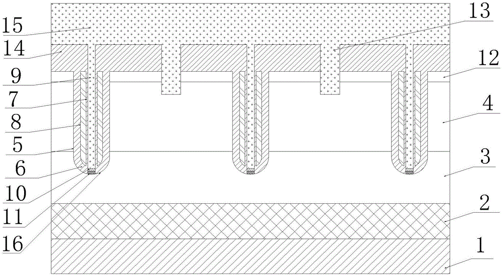
[0069] Such as image 3 As shown, the present invention provides a high-speed trench MOS device, including a first conductivity type drain region 1, an N+ single crystal silicon substrate 2 and an N- epitaxial layer located above the first conductivity type drain region 3. The P-type well region layer 4 located above the N- epitaxial layer 3, the N+ source region layer 12 located above the P-type well region layer 4, and the insulating medium located above the N+ source region layer 12 Layer 14, and the metal zone layer 15 located above the insulating dielectric layer 14, further ...


PUM


Abstract

The invention belongs to the technical field of semiconductor power device, specifically relates to a high-speed groove MOS device and preparing method thereof, integrates the Schottky diode structure into the groove of each groove MOSFET unit cell and forms the Schottky contact at the bottom of MOSFET unit cell groove, so as to effectively save the silicon surface area and reduce the chip cost. The device has simple manufacturing technology, low cost, new structure and high product performance and reliability, and can effectively restrain the peak voltage and peak current recovered reversely of the groove MOSFET device.

Description

technical field [0001] The invention belongs to the technical field of semiconductor device manufacturing, and in particular relates to a high-speed trench MOS device and a manufacturing method thereof. Background technique [0002] Trench MOSFET devices are widely used in power circuits as switching devices to connect power and loads. For a long time, how to reduce power loss and suppress the reverse recovery peak voltage and reverse recovery current of the MOS device's own parasitic diode has been the most concerned topic, especially in today's advocacy of energy saving, emission reduction and low carbon. [0003] Take the MOS tube in the DC-DC converter as an example, such as figure 1 As shown, it is a schematic diagram of a DC-DC conversion control circuit using a MOS tube as a switching device. It can be seen from the figure that the trench MOSFET devices M1 (upper tube) and M2 (lower tube) are the core switching devices of the circuit, and the DC-DC conversion is rea...

Claims


Application Information

Patent Timeline
Patent Type & Authority Applications(China)
IPC IPC(8): H01L27/07H01L29/78H01L21/8249
CPCH01L21/8249H01L27/0727H01L29/7827
Inventor 徐吉程袁力鹏范玮
Owner 华羿微电子股份有限公司
Why Eureka
Try Eureka