A kind of field effect transistor material based on multi-condensed rings and its preparation method and application

A field-effect transistor and transistor technology, which is applied in the manufacture of semiconductor/solid-state devices, electric solid-state devices, semiconductor devices, etc., can solve the problems of difficult adjustment of energy levels, short conjugate length, poor planarity, etc., to improve electron mobility, Good film-forming properties and reduced recombination energy

Active Publication Date: 2018-02-02
SUZHOU JOYSUN ADVANCED MATERIALS CO LTD
View PDF3 Cites 0 Cited by
  • Summary
  • Abstract
  • Description
  • Claims
  • Application Information

AI Technical Summary

Problems solved by technology

[0004] Technical problem to be solved: Aiming at the shortcomings of existing organic transistor materials, such as poor planarity, short conjugate length, poor solubility, and difficult adjustment of energy levels, the present invention provides a field effect transistor material based on multi-condensed rings, the transistor The material has the advantages of superior planar structure, long conjugate length, good solubility, and easy regulation of energy level.

Method used


Image

  • A kind of field effect transistor material based on multi-condensed rings and its preparation method and application
  • A kind of field effect transistor material based on multi-condensed rings and its preparation method and application
  • A kind of field effect transistor material based on multi-condensed rings and its preparation method and application

Examples


Embodiment 1

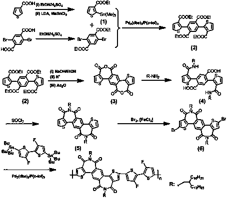
[0040] When X is an S atom, A is R is The prepared chemical structure is The preparation steps of the transistor material PIM-DTF with an n value of 1-100 are as follows:

[0041] (1) Synthesis of Compound 1: In a 250mL round-bottomed flask, 4.76g of diisopropylamine and 100mL of tetrahydrofuran were added under the protection of argon, the mixed solution was cooled to -78°C, and 19.2mL of n-butyllithium was added dropwise thereto Solution, after the dropwise addition, stirred at -78°C for 40min, then dissolved 6.01g of ethyl thiophene-3-carboxylate in 500mL of tetrahydrofuran and added dropwise to the mixed solution in the round bottom flask, after the dropwise addition, continued to stir After 1 hour, 46.1 mL of trimethyltin chloride was added dropwise. After 1 hour of reaction, the reaction liquid was heated to room temperature and stirred for 5 hours. After the reaction was completed, it was extracted with ethyl acetate, washed with water, dried with anhydrous sodium ...


PUM

PropertyMeasurementUnit
thermal decomposition temperatureaaaaaaaaaa

Abstract

A field effect transistor material based on polyfused rings and its preparation method and application, the chemical structural formula of the transistor material is: wherein the value of n is 1-100; X is selected from one of the following atoms: O, S , Se, Te; A is a group with a π-conjugated structure, selected from one of the following groups: R is selected from one of the following groups: the transistor material provided by the invention has high efficiency and is easy to prepare, and is compatible with Compared with the existing organic field effect materials, its own structure has better planarity, good film-forming properties, and easy adjustment of energy levels, thereby greatly improving charge mobility. The finished product can be used to make flexible electronic devices. Organic luminescence, organic photodetectors, organic solar cells, pressure sensors, organic storage devices, flexible electronic panels, electronic paper and many other fields have potential and broad application prospects.

Description

technical field [0001] The invention belongs to the field of field effect transistors, and in particular relates to a field effect transistor material based on multi-condensed rings and its preparation method and application. Background technique [0002] Organic Field Effect Transistors (OFETs) are the basic building blocks of organic circuits. They have the advantages of light weight, low cost, flexibility, and suitable for large-area preparation. They are widely used in organic sensors, organic memory devices, flexible flat panel displays, Electronic paper, radio frequency identification and many other fields have important application prospects. Transistor has achieved world-renowned development in the past half century and is one of the main cornerstones of modern electronics and microelectronics. With the further development of electronics in recent years, transistors are facing another revolution: the transition from traditional inorganic semiconductor transistors to...

Claims


Application Information

Patent Timeline
Patent Type & Authority Patents(China)
IPC IPC(8): C07D495/22C07D519/00C08G61/12H01L51/30H01L51/05
CPCC07D495/22C07D519/00C08G61/12C08G61/126C08G2261/344C08G2261/124C08G2261/3223H10K85/657H10K10/46Y02P20/582Y02E10/549
Inventor 廖良生李永玺吴福鹏
Owner SUZHOU JOYSUN ADVANCED MATERIALS CO LTD
Why Eureka
Try Eureka