Method of utilizing a built-in electric field in polar crystal to adjust and control separation efficiency and optic electrochemical activity of photon-generated carriers in photoelectrode of ZnO single crystal
A photoelectrode and electrochemical technology, which is applied in chemical instruments and methods, crystal growth, single crystal growth, etc., can solve the problem of limited improvement in the separation efficiency of photogenerated carriers, and achieve improved carrier separation efficiency and activity, The effect of simple preparation method and enhanced separation efficiency
- Summary
- Abstract
- Description
- Claims
- Application Information
AI Technical Summary
Problems solved by technology
Method used
Image
Examples
Embodiment 1
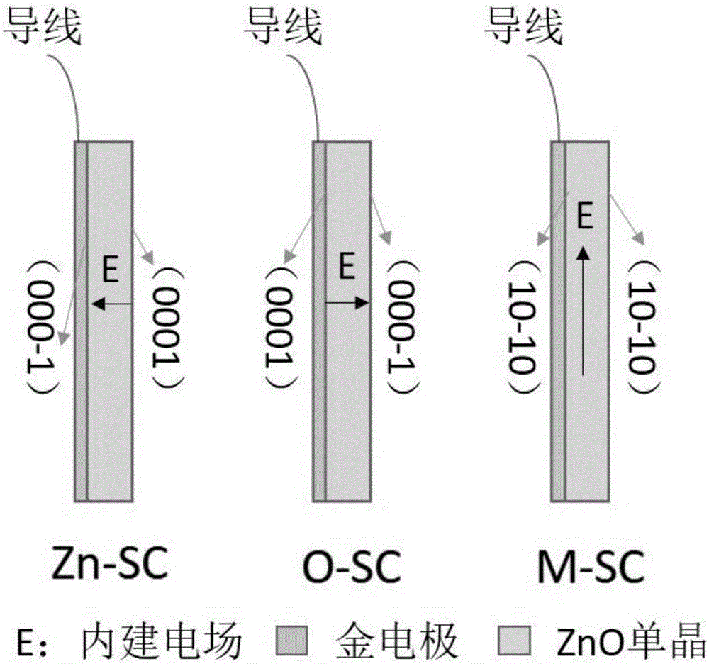
[0034] Process the C-cut and M-cut ZnO single crystal wafers to a thickness of 0.05-0.5 mm, and use H 3 PO 4 / CH 3 COOH / H 2 Soak the mixed solution of O (1:1:30, pH=1.3) for 5 minutes, wash with deionized water, and dry. Two C-cut ZnO single crystal wafers and M-cut ZnO single crystal wafers were respectively selected, and gold was sprayed on the (0001), (000-1) and (10-10) surfaces, and then the gold-sprayed ZnO single crystal wafers were heated at 500 °C Annealed for 10 minutes, and the ZnO single crystal electrode ( figure 1 ), the electrode is named after the exposed crystal plane of the non-sprayed gold surface, such as: the electrodes with exposed crystal planes of (0001), (000-1) and (10-10) planes are named: Zn-SC, O-SC and M -SC. The direction of the electric field inside the electrode is figure 1 The direction pointed by the black tip, in Zn-SC, the direction of the built-in electric field is perpendicular to the electrode surface and points to the Au electrode...
Embodiment 2
[0039] Process the C-cut and M-cut ZnO single crystal wafers to a thickness of 0.05-0.5 mm, and use H 3 PO 4 / CH 3 COOH / H 2 Soak the mixed solution of O (1:1:30, pH=1.3) for 1 to 10 minutes, wash with deionized water, and dry. Two C-cut ZnO single crystal wafers and M-cut ZnO single crystal wafers were respectively selected, and gold was sprayed on the (0001), (000-1) and (10-10) surfaces, and then the gold-sprayed ZnO single crystal wafers were heated at 510 °C Annealed for 1 minute, and the wire was drawn out on the gold-sprayed surface to prepare a ZnO single crystal electrode ( figure 1 ), the electrode is named after the exposed crystal plane of the non-sprayed gold surface, such as: the electrodes with exposed crystal planes of (0001), (000-1) and (10-10) planes are named: Zn-SC, O-SC and M -SC. The direction of the electric field inside the electrode is figure 1 The direction pointed by the black tip, in Zn-SC, the direction of the built-in electric field is perpe...
Embodiment 3
[0044] Process the C-cut and M-cut ZnO single crystal wafers to a thickness of 0.05-0.5 mm, and use H 3 PO 4 / CH 3 COOH / H 2 Soak the mixed solution of O (1:1:30, pH=1.3) for 1 to 10 minutes, wash with deionized water, and dry. Two C-cut ZnO single crystal wafers and M-cut ZnO single crystal wafers were respectively selected, and gold was sprayed on the (0001), (000-1) and (10-10) surfaces, and then the gold-sprayed ZnO single crystal wafers were heated at 505 °C Annealed for 5 minutes, and the ZnO single crystal electrode ( figure 1 ), the electrode is named after the exposed crystal plane of the non-sprayed gold surface, such as: the electrodes with exposed crystal planes of (0001), (000-1) and (10-10) planes are named: Zn-SC, O-SC and M -SC. The direction of the electric field inside the electrode is figure 1 The direction pointed by the black tip, in Zn-SC, the direction of the built-in electric field is perpendicular to the electrode surface and points to the Au elec...
PUM
 Abstract
Description
Claims
Application Information


