Manufacturing method of ohmic contact electrode based on AlGaN/GaN HEMT

A technology of ohmic contact electrodes and electrodes, applied in semiconductor/solid-state device manufacturing, circuits, electrical components, etc., can solve problems such as low reliability, inability to form good ohmic contacts, high heat, etc.

Inactive Publication Date: 2017-02-01
PEKING UNIV FOUNDER GRP CO LTD +1
View PDF6 Cites 6 Cited by
  • Summary
  • Abstract
  • Description
  • Claims
  • Application Information

AI Technical Summary

Problems solved by technology

[0004] In order to reduce the ohmic contact resistance of AlGaN / GaN HEMT devices, in the prior art, before depositing the ohmic electrode metal layer, the method of using hydrogen chloride solution to remove atoms and ionic impurities on the surface of the AlGaN barrier layer is used to reduce the ohmic contact resistance. The presence of other substances on the surface of the AlGaN barrier layer cannot form a good ohmic contact, resulting in a high ohmic contact resistance of the AlGaN / GaN HEMT device, which in turn makes the AlGaN / GaN HEMT device generate higher heat and lower reliability

Method used


Image

  • Manufacturing method of ohmic contact electrode based on AlGaN/GaN HEMT
  • Manufacturing method of ohmic contact electrode based on AlGaN/GaN HEMT
  • Manufacturing method of ohmic contact electrode based on AlGaN/GaN HEMT

Examples


Embodiment 1

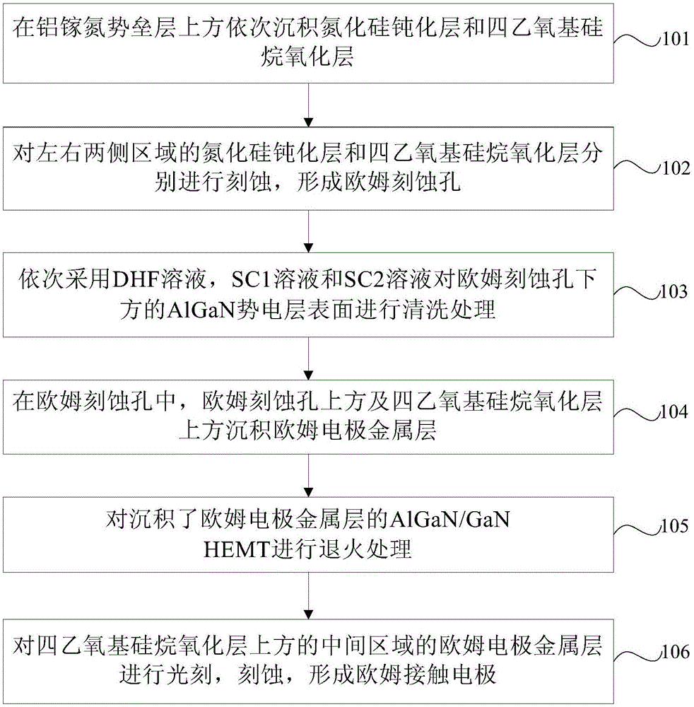
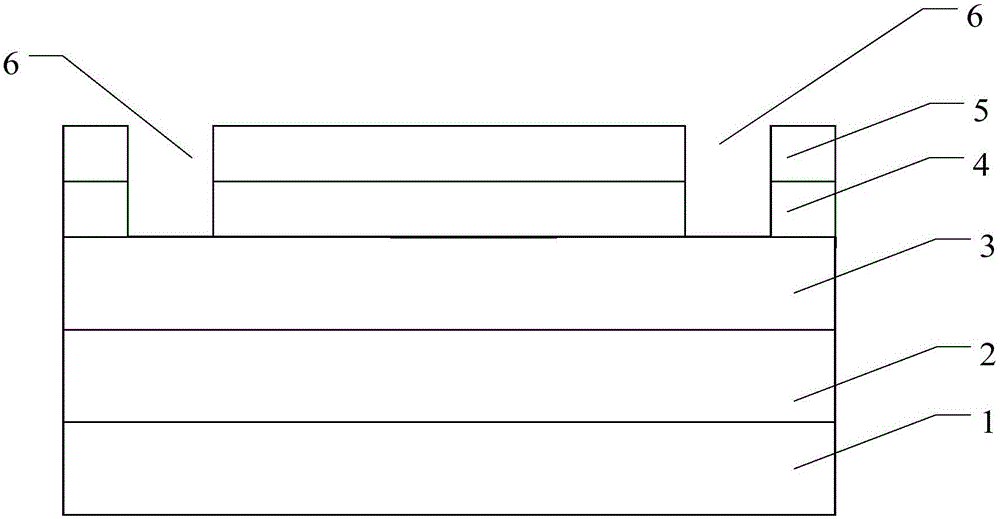
[0039] figure 1 It is a flow chart of Embodiment 1 of the manufacturing method of the ohmic contact electrode based on AlGaN / GaN HEMT of the present invention, as figure 1 As shown, the manufacturing method of the AlGaN / GaN HEMT-based ohmic contact electrode provided in this embodiment includes:

[0040] Step 101 , depositing a silicon nitride passivation layer 4 and a tetraethoxysilane oxide layer 5 sequentially on the AlGaN barrier layer 3 .

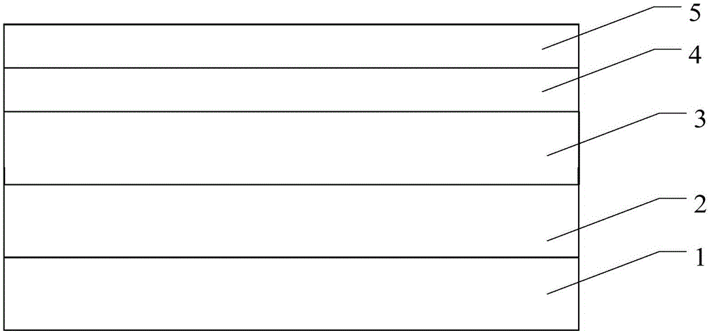
[0041] In this example, figure 2 It is a schematic diagram of the structure after sequentially depositing a silicon nitride passivation layer and a tetraethoxysilane oxide layer on the AlGaN barrier layer in the method for manufacturing an ohmic contact electrode based on AlGaN / GaN HEMT provided by Embodiment 1 of the present invention, Such as figure 2 As shown, a silicon nitride passivation layer (abbreviation: SiN passivation layer) 4 and a tetraethoxysilane oxide layer (abbreviation: TEOS oxidation layer) are sequentially depo...


PUM

PropertyMeasurementUnit
thicknessaaaaaaaaaa
thicknessaaaaaaaaaa

Abstract

The invention provides a manufacturing method of an ohmic contact electrode based on an AlGaN/GaN HEMT. The method comprises the following stesp: successively depositing a silicon nitride passivation layer and a tetraethoxysilane oxide layer above an aluminum gallium nitride barrier layer; etching the silicon nitride passivation layer and the tetraethoxysilane oxide layer at a left-side area and a right-side area to form ohmic etching holes; performing cleaning processing on the aluminum gallium nitride barrier layer below the ohmic etching holes successively by use of a DHF solution, an SC1 solution and an SC2 solution; in the ohmic etching holes, depositing an ohmic electrode metal layer above the ohmic etching holes and the tetraethoxysilane oxide layer, and performing annealing processing on the AlGaN/GaN HEMT with the ohmic electrode metal layer deposited thereon; and performing photoethcing and etching on the ohmic electrode metal layer at an intermediate area above the tetraethoxysilane oxide layer so as to form the ohmic contact electrode. According to the invention, good ohmic contact is formed between the ohmic electrode contact layer and the aluminum gallium nitride barrier layer, and thus ohmic contact resistance of a device is effectively reduced.

Description

technical field [0001] Embodiments of the present invention relate to the technical field of semiconductor device manufacturing, and in particular to a method for manufacturing an ohmic contact electrode based on AlGaN / GaN HEMT. Background technique [0002] AlGaN / GaN is a new type of wide bandgap compound semiconductor material that is widely concerned in the world. Because of its wide bandgap width, high electron saturation drift rate, high breakdown field strength, good thermal stability, corrosion resistance and Anti-radiation performance, so it has strong advantages in high-voltage, high-frequency, high-temperature, high-power and anti-radiation environmental conditions. With its excellent material properties, AlGaN / GaN high electron mobility transistors (abbreviation: AlGaN / GaN HEMTs) are widely used. [0003] However, due to the wide band gap of GaN material in AlGaN / GaN HEMT and the use of AlGaN non-doped intrinsic material, the ohmic contact resistance in AlGaN / GaN...

Claims


Application Information

Patent Timeline
Patent Type & Authority Applications(China)
IPC IPC(8): H01L21/28H01L21/283H01L29/778
CPCH01L21/28H01L21/283H01L29/7786
Inventor 刘美华陈建国李杰
Owner PEKING UNIV FOUNDER GRP CO LTD
Why Eureka
Try Eureka