A CMOS Broadband Low Noise Amplifier with Adjustable Gain

A broadband low-noise, amplifier technology, applied in the field of CMOS broadband low-noise amplifier, achieves the effect of clear circuit structure principle, guaranteed noise figure, and reduced chip area

Inactive Publication Date: 2019-04-16
CHINA JILIANG UNIV
View PDF10 Cites 0 Cited by
  • Summary
  • Abstract
  • Description
  • Claims
  • Application Information

AI Technical Summary

Problems solved by technology

[0007] Aiming at the above-mentioned technical defects existing in the prior art, the present invention provides a CMOS broadband low-noise amplifier with adjustable gain. The circuit structure is composed of MOS transistors, capacitors and resistors. There is no integrated inductor, which greatly reduces the chip area, and can also ensure a certain noise figure in the case of adjustable gain

Method used


Image

  • A CMOS Broadband Low Noise Amplifier with Adjustable Gain
  • A CMOS Broadband Low Noise Amplifier with Adjustable Gain
  • A CMOS Broadband Low Noise Amplifier with Adjustable Gain

Examples


Embodiment Construction

[0025] In order to describe the present invention more specifically, the technical solutions of the present invention will be described in detail below in conjunction with the accompanying drawings and specific embodiments.

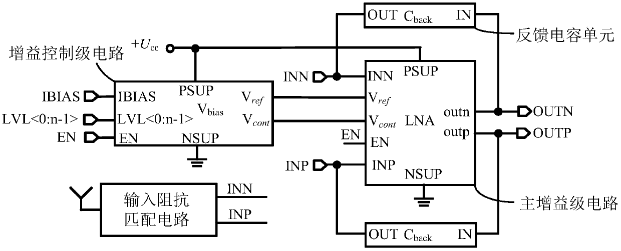
[0026] Such as figure 1 As shown, the CMOS broadband low-noise amplifier with adjustable gain of the present invention includes an input impedance matching circuit, a main gain stage circuit, a gain control stage circuit and a feedback capacitance unit; wherein

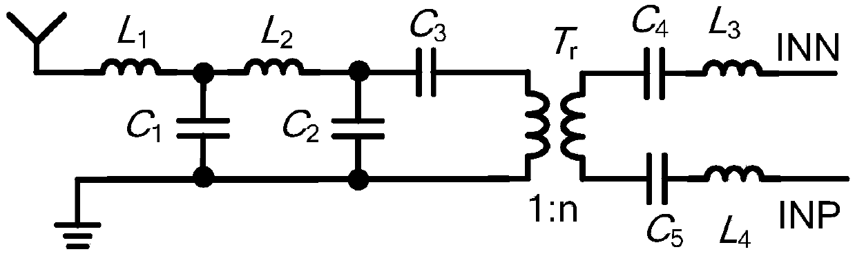
[0027] The input impedance matching circuit receives the RF input signal from the antenna or other equipment, and is directly connected to the main gain stage circuit, which converts the single-ended signal input by the antenna into a pair of differential signals, so that the broadband low-noise amplifier can operate at the set frequency range to meet the input impedance matching requirements. Such as figure 2 As shown, the input impedance matching circuit in this embodiment includes five capa...


PUM


Abstract

The invention discloses a gain-adjustable CMOS (Complementary Metal-Oxide-Semiconductor Transistor) broadband low-noise amplifier. The gain-adjustable CMOS broadband low-noise amplifier comprises a main gain grade circuit, an input impedance matching circuit, a gain control grade circuit and a feedback capacitance unit. According to the gain-adjustable CMOS broadband low-noise amplifier, programmable voltage is generated through controlling conduction of a tail current source; the programmable voltage is applied to a grid electrode of a common-gate tube of the main gain grade circuit, and transconductance of the common-gate tube is changed, so that grid source voltage of a common-source tube is changed, and the transconductance of the common-source tube is changed, furthermore, a transconductance sum of the common-gate and common-source tubes of an input grade is changed; finally, input matching is changed to generate different amplification gains; meanwhile, a feedback capacitance which is output to input is introduced to compensate the input matching when regulating voltage is different; accurate gain stepping of broadband matching and low-noise amplifiers can be realized through reasonably planning the programmable voltage and the feedback capacitance.

Description

technical field [0001] The invention belongs to the technical field of CMOS integrated circuits, and in particular relates to a gain-adjustable CMOS broadband low-noise amplifier. Background technique [0002] Wireless communication is one of the fastest growing technologies today. In the past ten years, with the rapid development of personal communication systems, digital TV, and broadcasting, people's research on RF front-end transceivers has entered a white-hot state. Due to the continuous increase in the amount of communication data, multi-mode, multi-frequency and broadband communication is gradually becoming a trend. Multi-mode multi-frequency receivers need to be compatible with multiple frequency points and have a wide frequency coverage. This puts forward higher requirements for the low-noise amplifier of the ultra-wideband receiver, requiring noise matching and signal low-noise amplification at multi-mode and multi-frequency points. At the same time, with the de...

Claims


Application Information

Patent Timeline
Patent Type & Authority Patents(China)
IPC IPC(8): H03F3/16H03F1/26H03F1/56H03G3/30
CPCH03F1/26H03F1/565H03F3/165H03G3/30H03G2201/307
Inventor 吴秀山韩建强俞丙威王艳智
Owner CHINA JILIANG UNIV
Why Eureka
Try Eureka