Active optical phased array photon integration chip and manufacturing method thereof

A photon integration, phased array technology, applied in lasers, laser devices, phonon exciters, etc., can solve the problems of difficult injection locking of injected optical power, and no simultaneous locking of multiple laser output phases.

Active Publication Date: 2017-02-15
TSINGHUA UNIV
View PDF3 Cites 33 Cited by
  • Summary
  • Abstract
  • Description
  • Claims
  • Application Information

AI Technical Summary

Problems solved by technology

[0006] However, although someone has proposed the idea of ​​realizing a coherent laser array, so far, no experimental reports or products have been seen in which one laser simultaneously locks the output phases of multiple lasers.
The fundamental problem here is that those who have really been engaged in the research of laser injection locking know that the realization of laser injection locking cannot be achieved by just entering the laser light of one laser into another laser. The free working frequency of the slave laser before being locked must be very close to the master laser. It is possible to find the locking possibility only when the operating frequency is high, and the lower the injection optical power is, the more difficult it is to achieve injection locking

Method used


Image

  • Active optical phased array photon integration chip and manufacturing method thereof
  • Active optical phased array photon integration chip and manufacturing method thereof

Examples


Embodiment 1

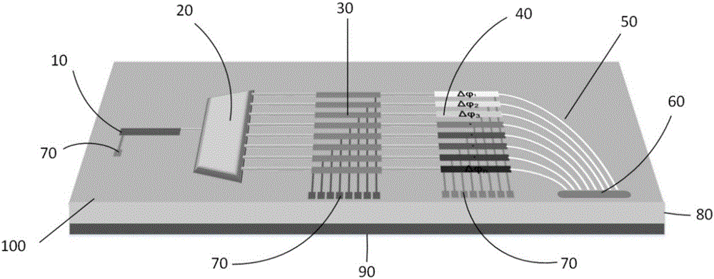
[0050] The active optical phased array photonic integrated chip 100 with an operating wavelength range of 1.3 μm˜2.0 μm may be based on the same InP substrate 80 . The substrate 80 is either highly doped n-InP, and the back electrode 90 is located on the back of the substrate 80 ; or is semi-insulating InP, and the back electrode 90 is located on the front of the substrate 80 .

[0051] The semiconductor epitaxial structure, waveguide structure and wavelength selection structure of the master laser 10 and the slave laser array 30 are the same. The semiconductor epitaxial structure adopts p-i-n structure, the p and n layers can use InP or AlInAs, the thickness range is 1-2μm, and the i layer can use InGaAs, InGaAsP, AlGaInAs and other ternary or quaternary alloy III-V compound semiconductor multiple quantum wells structure, the corresponding emission spectrum peak ranges from 1.2 μm to 2.0 μm, and the thickness ranges from 0.05 to 0.5 μm.

[0052] Laser wavelength or frequency...

Embodiment 2

[0059] The active optical phased array photonic integrated chip 100 with an operating wavelength range of 0.6 μm˜1.1 μm may be based on the same GaAs or GaP substrate 80 . The substrate 80 is either a highly doped substrate, and the back electrode 90 is located on the back of the substrate 80 ; or is a semi-insulating substrate, and the back electrode 90 is located on the front of the substrate 80 .

[0060] The semiconductor epitaxial structure, waveguide structure, and wavelength selection structure of the master laser 10 and the slave laser array 30 are the same, the semiconductor epitaxial structure adopts a p-i-n structure, the p and n regions can use GaAlAs or GaInP, and the thickness range is 0.2-2 μm, and the i region can use GaAlAs , AlGaInP and other ternary or quaternary alloy III-V compound semiconductors, the corresponding emission spectrum peak range is 0.6 μm to 1.1 μm, and the thickness range is 0.05 to 0.5 μm.

[0061] Laser wavelength or frequency selection i...

specific Embodiment approach

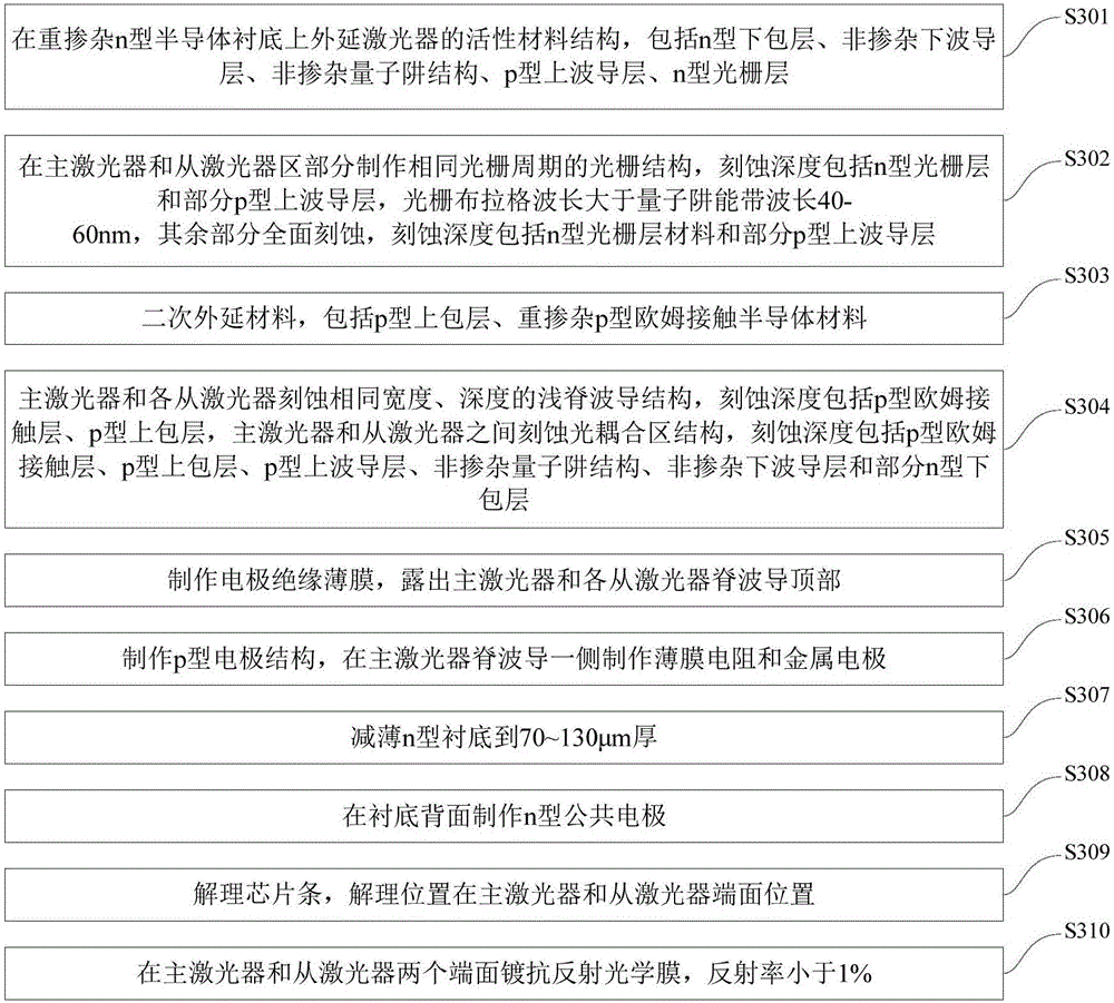
[0083] In a specific embodiment of the present invention, a method for preparing an active optical phased array photonic integrated chip with a wavelength of about 1550 nm is taken as an example. The active optical phased array photonic integrated chip includes a master laser, an optical isolation coupling region, a slave laser array, an optical phase modulator array, a transition waveguide array, an optical field radiation array, a positive electrode, a substrate and a back electrode. All devices use the same epitaxial structure. The specific implementation is as follows:

[0084] On a highly doped n-type InP substrate, the following materials are grown by metal organic chemical vapor phase epitaxy (MOVPE): n-type InP buffer layer (thickness 1000nm, doping concentration about 1×10 18 cm -3 ), i-layer 400nm, including undoped lattice matching InGaAsP lower waveguide layer (thickness 100nm, optical fluorescence wavelength 1150nm), InGaAsP active layer multiple quantum wells (...


PUM


Abstract

The invention discloses an active optical phased array photon integration chip and a manufacturing method thereof. The chip comprises a coherent laser array, an optical phase modulator array, a transitional waveguide array and a light field radiation array, wherein the coherent laser array is a master-slave laser realized through a same material and a same technology; through a unidirectional injection locking mode, a plurality of slave lasers possess a same frequency and good coherence of a fixed phase; the optical phase modulator array controls phase delay of each optical phase modulator in the plurality of optical phase modulators to light through an electric signal modulation mode; and the transitional waveguide array and the light field radiation array are used for adjusting wave beams and emission positions of coherent beams which are emitted from different lasers, pass through different optical phase modulators and possess different optical phase delays and determining a coherent superposed light beam emitting direction according to differences of the phase delays. The integration chip can be integrated on a same substrate. Total power of output light is formed by coherent superposition of slave lasers. And the chip possesses advantages of chip integration and high emitting power.

Description

technical field [0001] The invention relates to the technical field of semiconductors, in particular to an active optical phased array photonic integrated chip and a preparation method thereof. Background technique [0002] In related technologies, lidar uses laser light instead of radio waves as the emission source, which has the advantages of small size and high detection accuracy compared with traditional radar. From the initial simple ranging to the current three-dimensional imaging, lidar has a wide range of applications in various military and civilian occasions. [0003] Limited by the number of lasers that can be integrated, in order to obtain high-resolution 3D radar images, lidar needs to add a scanning device after the laser. Existing commercial LiDAR uses a mechanical scanning device to change the direction of the laser beam, which has the disadvantages of slow scanning and imaging speed, large weight and volume. If the outgoing direction of the laser beam can ...

Claims


Application Information

Patent Timeline
Patent Type & Authority Applications(China)
IPC IPC(8): H01S5/125H01S5/06H01S5/062H01S5/0625H01S5/40
CPCH01S5/06246H01S5/06256H01S5/125H01S5/40
Inventor 罗毅熊兵王健郝智彪孙长征李洪涛韩彦军汪莱
Owner TSINGHUA UNIV
Why Eureka
Try Eureka