Three-dimensional infrared detector pixel structure and preparation method therefor

An infrared detector and infrared detection technology, applied in the direction of resistors, resistance manufacturing, electrical components, etc., can solve the problems of low sensitivity, expensive materials, complex detection process, etc., achieve flexible setting positions, increase integration density, The effect of increasing the fill factor

Active Publication Date: 2017-02-22
SHANGHAI INTEGRATED CIRCUIT RES & DEV CENT
View PDF2 Cites 0 Cited by
  • Summary
  • Abstract
  • Description
  • Claims
  • Application Information

AI Technical Summary

Problems solved by technology

[0003] However, the sensitivity of the detector structure using thermal elements is usually not very high, and the structure is relatively complicated, and the detection process is complicated. If a thermal sensor with high sensitivity is used, the material cost is expensive;

Method used


Image

  • Three-dimensional infrared detector pixel structure and preparation method therefor
  • Three-dimensional infrared detector pixel structure and preparation method therefor
  • Three-dimensional infrared detector pixel structure and preparation method therefor

Examples


Embodiment 1

[0060] The following is attached Figures 1a-8c The present invention will be described in further detail with specific examples. It should be noted that the drawings are all in a very simplified form, using imprecise scales, and are only used to facilitate and clearly achieve the purpose of assisting in describing the present embodiment.

[0061] It should be noted that, in this embodiment, the surface of the silicon substrate also has a reflection area, the reflection area is located below the infrared detection structure, and there is a dielectric layer between the reflection area and the conductive metal area; the interconnection layer is connected to the external circuit. The infrared detection structure adopts the micro bridge structure. The conductive layer is a conductive metal layer.

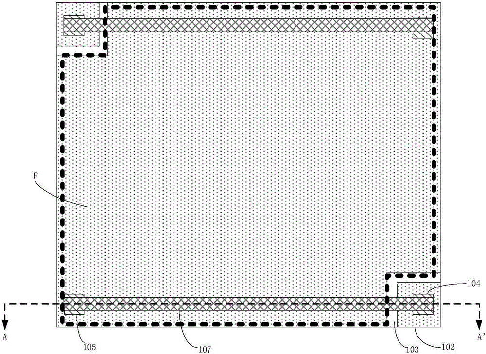
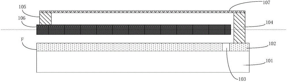
[0062] For this example, see Figure 1a with Figure 1b , Figure 1b for along Figure 1a Schematic diagram of the cross-sectional structure of AA', Figure 1a In the figure, for th...

Embodiment 2

[0092] The following is attached Figure 8a-14 The present invention will be described in further detail with specific examples. It should be noted that the drawings are all in a very simplified form, using imprecise scales, and are only used to facilitate and clearly achieve the purpose of assisting in describing the present embodiment.

[0093] For this example, see Figure 9a with Figure 9b , Figure 9b for along Figure 9a Schematic diagram of the cross-sectional structure of the middle BB', Figure 9aIn the figure, for the sake of convenience, the micro-bridge structure is removed, and the area occupied by the micro-bridge structure is represented by a thick dotted line frame. The infrared detector pixel structure is located on a silicon substrate 201, and the silicon substrate 201 has an interconnection layer (not shown) shown), the surface of the silicon substrate 201 has a conductive metal region 202 electrically connected to the interconnection layer, a reflecti...

Embodiment 3

[0115] The following is attached Figures 15a-21 The present invention will be described in further detail with specific examples. It should be noted that the drawings are all in a very simplified form, using imprecise scales, and are only used to facilitate and clearly achieve the purpose of assisting in describing the present embodiment.

[0116] For this example, see Figure 15a with Figure 15b , Figure 15b for along Figure 15a Schematic diagram of CC' section structure, Figure 15a In , for the convenience of representation, the micro-bridge structure is removed, and the area occupied by the micro-bridge structure is indicated by a thick dotted line frame. The infrared detector pixel structure is located on a silicon substrate 301, which has an interconnection layer, and the silicon substrate 301 has an interconnection layer. The surface of the substrate 301 has a conductive metal region 302 electrically connected to the interconnection layer, a reflective region 3...


PUM


Abstract

The invention provides a three-dimensional infrared detector pixel structure and a preparation method therefor. The three-dimensional infrared detector pixel structure comprises a conductive metal region, an infrared detection structure and a conductive beam structure, wherein the conductive metal region is located on the surface of a silicon substrate; the infrared detection structure is positioned above the silicon substrate and used for detecting infrared light and generating an electric signal; the conductive beam structure is electrically connected with the infrared detection structure and used for transmitting the electric signal generated by the infrared detection structure to the conductive metal region; the conductive beam structure comprises at least one layer of conductive beams and multiple layers of conductive trenches arranged in a vertical direction; the two ends of the conductive beams in each layer are in contact with two layers of conductive trenches, the bottoms of which are not positioned on the same plane; the infrared detection structure is in contact with one corresponding layer of the conductive trenches or the conductive beams; the conductive metal region is in contact with the bottoms of the other layer of the conductive trenches; and the electric signal generated by the infrared detection structure is transmitted in the height direction of the conductive trenches and in the horizontal direction of the conductive beams so as to be transmitted downwardly to the conductive metal region along a roundabout path in the vertical direction.

Description

technical field [0001] The invention relates to the technical field of semiconductors, in particular to a three-dimensional infrared detector pixel structure and a preparation method thereof. Background technique [0002] The infrared detector is a device that converts the incident infrared radiation signal into an electrical signal output. It uses a thermal element to detect the existence or movement of an object. The infrared radiation outside the detector mobile phone is then gathered on the infrared sensor. The infrared sensor uses a thermal element , the thermal element will output a signal when it receives a change in the temperature of the infrared radiation, convert it into an electrical signal, and then analyze the waveform of the electrical signal. Only one type of thermistor is used in the pixel structure of traditional infrared detectors, usually amorphous silicon or vanadium oxide with negative temperature coefficient, and the changing signal is amplified and ou...

Claims


Application Information

Patent Timeline
Patent Type & Authority Applications(China)
IPC IPC(8): H01C7/04H01C17/075H01C17/28
CPCH01C7/041H01C17/075H01C17/288
Inventor 康晓旭
Owner SHANGHAI INTEGRATED CIRCUIT RES & DEV CENT
Why Eureka
Try Eureka