Si/TiOx heterojunction-based double-sided crystalline silicon solar cell

A technology of solar cells and crystalline silicon, which is applied in the field of solar cells and semiconductor devices, can solve problems such as hindering the development of HIT solar cells and waste of production equipment, and achieve the effects of reducing photovoltaic power generation costs, increasing power generation, and enhancing built-in electric fields

Active Publication Date: 2017-02-22
NANCHANG UNIV
View PDF8 Cites 7 Cited by
  • Summary
  • Abstract
  • Description
  • Claims
  • Application Information

AI Technical Summary

Problems solved by technology

However, the production process and equipment of HIT cells are quite different from those of traditional silicon solar cells.
If the production of HIT solar cells is switched from traditional crystalline silicon solar cells, the current production equipment will be wasted
In addition, due to the need for expensive vacuum equipment in the production of HIT solar cells, the investment in a production line of the same scale is several times that of a traditional crystalline silicon solar cell production line
These hinder the development of HIT solar cells to a certain extent

Method used


Image

  • Si/TiOx heterojunction-based double-sided crystalline silicon solar cell

Examples


Embodiment 1

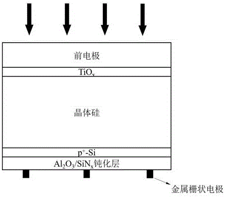
[0019] (1) Use n-type silicon wafers as the absorbing layer, conduct preliminary cleaning on the silicon wafers, and make texture on both sides.

[0020] (2) Prepare a p-type heavily doped layer on the back of the silicon wafer using a diffusion process.

[0021] (3) Deposit Al on the back 2 o 3 passivation layer, followed by grid-shaped Ag electrodes.

[0022] (4) Perform secondary cleaning on the front side of the silicon wafer.

[0023] (5) Preparation of TiO on the front side of the silicon wafer using atomic layer deposition x Floor.

[0024] (6) on TiO x An ITO transparent conductive layer and an Ag metal grid line are deposited on the layer to prepare a front electrode.

Embodiment 2

[0026] (1) Use p-type silicon wafers as the absorbing layer, conduct preliminary cleaning on the silicon wafers, and make texture on both sides.

[0027] (2) The p-type heavily doped layer on the back is prepared by ion implantation process.

[0028] (3) Deposit Al on the back 2 o 3 / SiN x passivation layer, followed by the fabrication of grid-like Cu electrodes.

[0029] (4) Perform secondary cleaning on the front side of the silicon wafer.

[0030] (5) Preparation of TiO by chemical vapor deposition on the front side of the silicon wafer x Floor.

[0031] (6) on TiO x An ITO transparent conductive layer and an Ag metal grid line are deposited on the layer to prepare a front electrode.


PUM


Abstract

The invention provides an Si / TiOx heterojunction-based double-sided crystalline silicon solar cell, which comprises a front electrode, a TiOx layer, a crystalline silicon absorption layer, a p-type crystalline silicon heavily doped layer, a passivation layer and a metal gate electrode, wherein the structure of the Si / TiOx heterojunction-based double-sided crystalline silicon solar cell is the front electrode, the TiOx layer, the crystalline silicon absorption layer, the p-type crystalline silicon heavily doped layer, the passivation layer and the metal gate electrode in sequence from a light facing surface; and an n-type doped TiOx and crystalline silicon are utilized by the light facing surface to form a heterojunction while a traditional crystalline silicon preparation technology based on diffusion is utilized by a back surface. The TiOx can well passivate the surface of a silicon wafer, and the TiOx and silicon form a good heterojunction, so that improvement of the open-circuit voltage and the conversion efficiency of the heterojunction cell is facilitated. Existing crystalline silicon solar cell production equipment can be fully utilized by a traditional crystalline silicon preparation technology of the back surface. The sunlight can be fully utilized by the double-sided structure; the actual generating capacity is increased; and the photovoltaic power generation cost is reduced.

Description

technical field [0001] The invention belongs to the field of solar cells and the field of semiconductor devices, and relates to the structural design of silicon solar cells. Background technique [0002] Crystalline silicon solar cells are an important type of solar cells, and their output accounts for most of the current total output of solar cells. With the advancement of technology, the photoelectric conversion efficiency of homogeneous crystalline silicon solar cells prepared based on diffusion technology is gradually approaching the limit. The heterojunction solar cell can make full use of the difference in work function and energy band position between two different semiconductors, and can enhance the built-in electric field strength without increasing the recombination of carriers inside the solar cell, thereby improving the photoelectricity of the solar cell. conversion efficiency. Therefore, crystalline silicon solar cells based on heterojunctions are expected to ...

Claims


Application Information

Patent Timeline
Patent Type & Authority Applications(China)
IPC IPC(8): H01L31/072H01L31/074H01L31/0352H01L31/0216
CPCY02E10/50H01L31/072H01L31/02168H01L31/0352H01L31/074
Inventor 高超黄海宾周浪岳之浩
Owner NANCHANG UNIV
Why Eureka
Try Eureka