

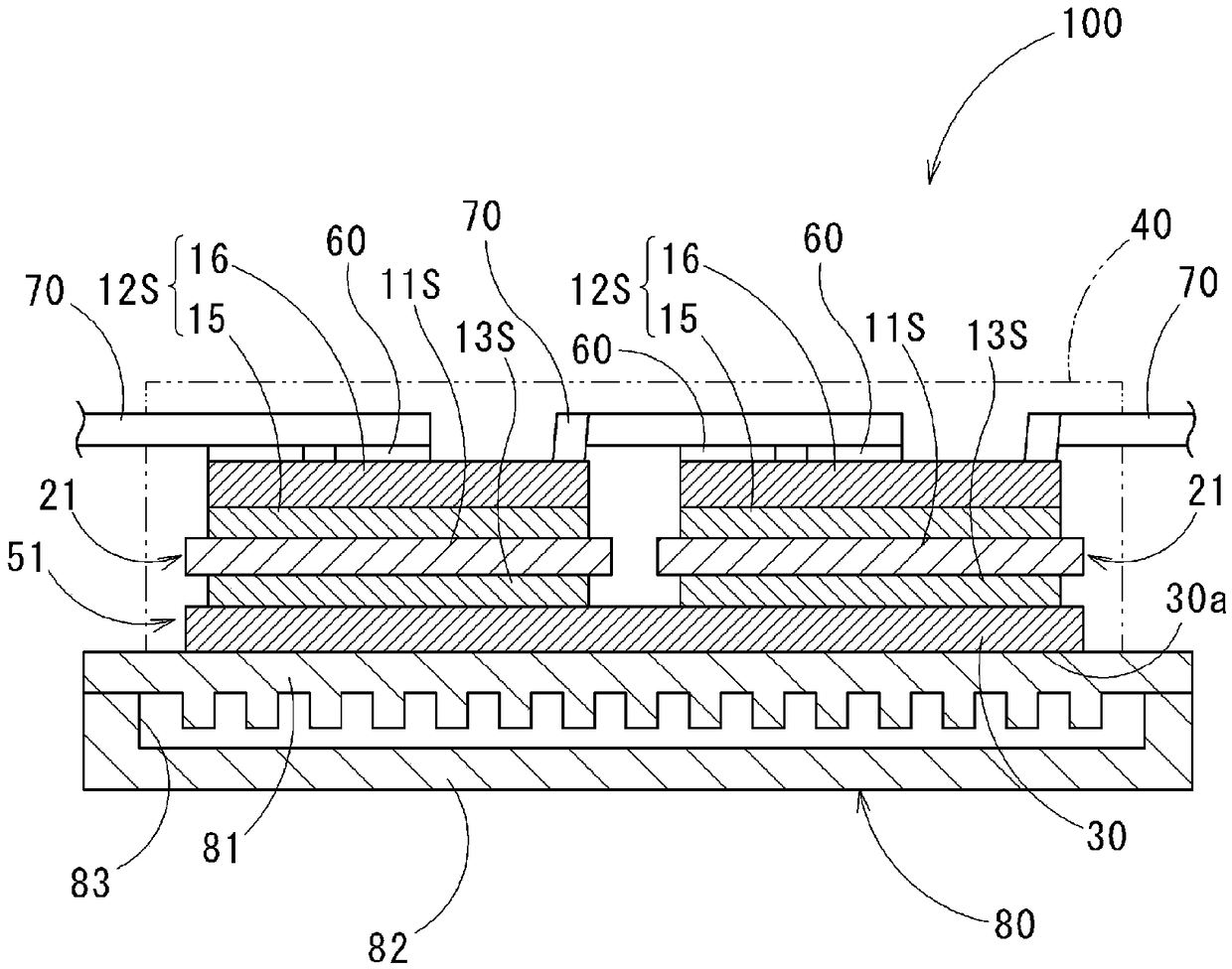
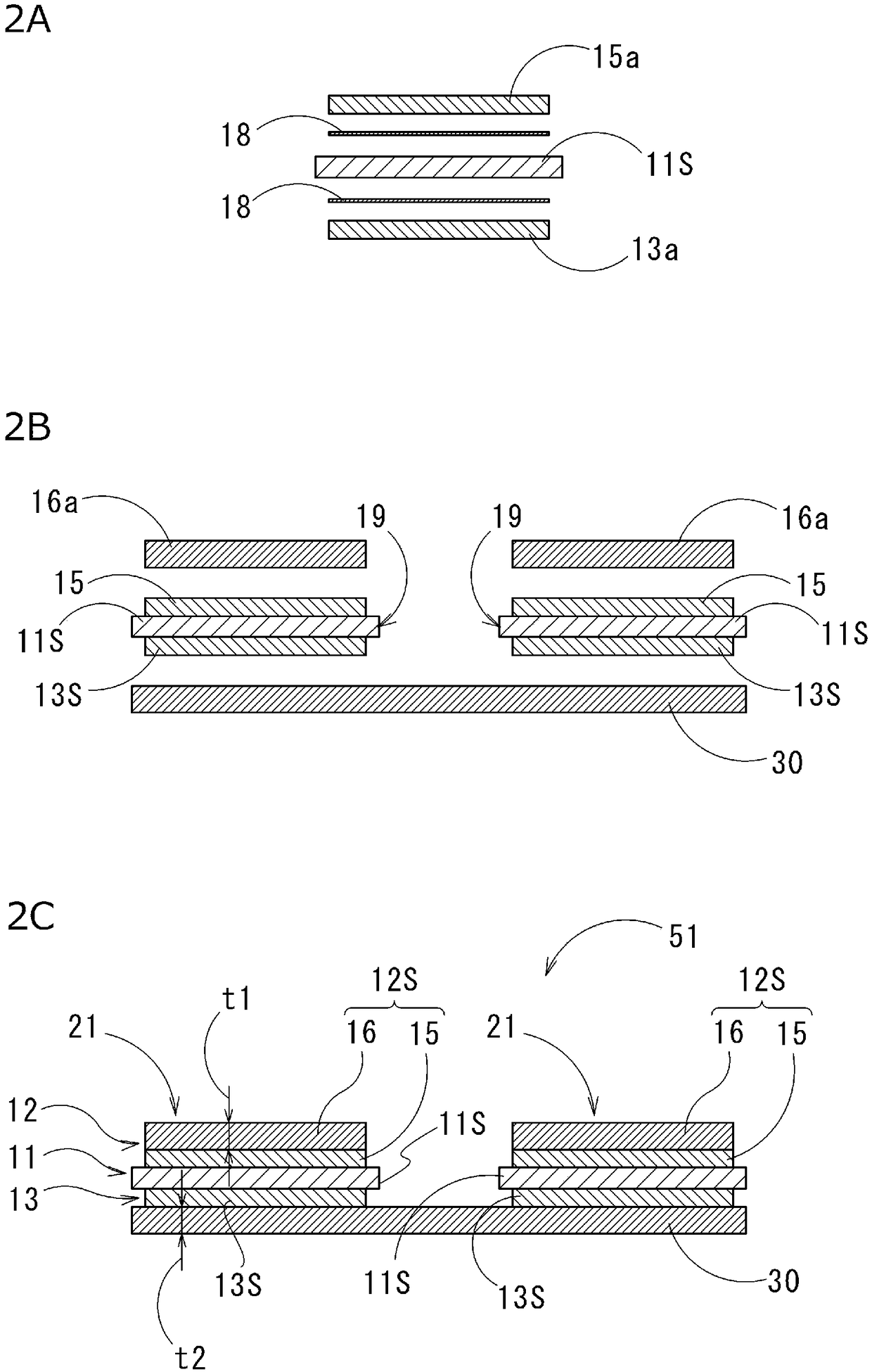
Power module base unit and power module
A technology of power modules and substrates, which is applied in the direction of electrical components, circuits, and electric solid-state devices, can solve the problems that it is difficult to accurately locate multiple insulating substrates, it is difficult to obtain the position accuracy of insulating substrates, and it is difficult to achieve integration. Achieve high integration, improve connection reliability, and good heat dissipation
- Summary
- Abstract
- Description
- Claims
- Application Information
AI Technical Summary
Problems solved by technology
Method used
Image

Examples
Embodiment
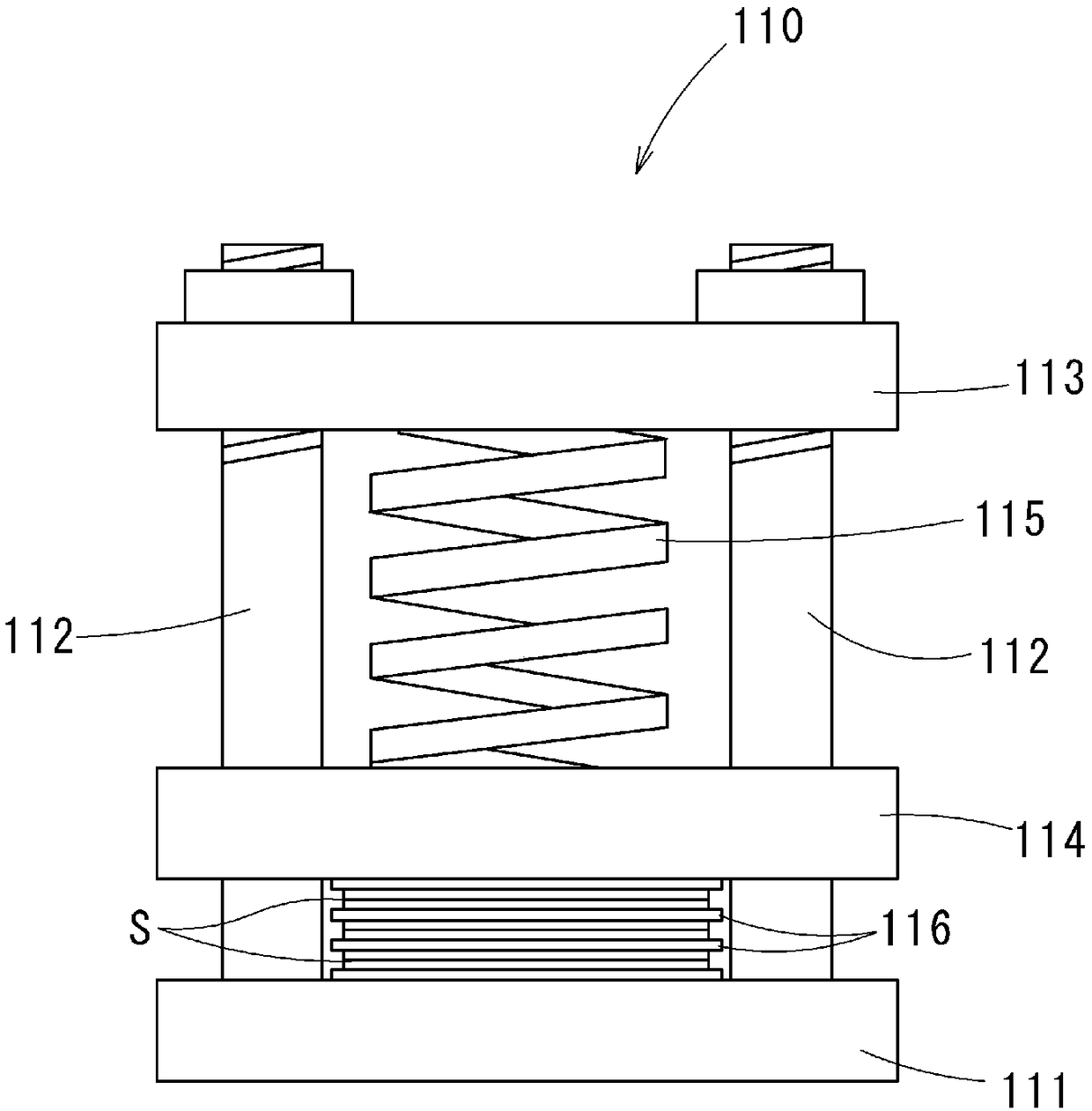
[0088] Next, examples performed to confirm the effects of the present invention will be described.
[0089] As a sample of the substrate unit for a power module, a ceramic substrate composed of AlN with a thickness of 0.635 mm was prepared as a ceramic substrate layer, and a 0.6 mm-thick aluminum plate with a purity of 99.99 Aluminum plate with mass % or more (4N). Pass C1020 (yield strength = 195N / mm 2 ) or heat-resistant alloy ZC manufactured by Mitsubishi Shindoh Co., Ltd. (yield strength = 280N / mm 2 ), prepare plates with the thicknesses shown in Table 1. In addition, the value of yield strength is the value at room temperature (25 degreeC). The planar dimensions of each component were formed as shown in Table 1.
[0090] These were joined by the joining method described in the said embodiment, and the sample of the board|substrate unit for power modules was produced. "Embodiment" in Table 1 indicates which embodiment of the production method each sample was produced ...
PUM
| Property | Measurement | Unit |
|---|---|---|
| thickness | aaaaa | aaaaa |
| thickness | aaaaa | aaaaa |
| thickness | aaaaa | aaaaa |
Abstract
Description
Claims
Application Information