Unlock instant, AI-driven research and patent intelligence for your innovation.

Manufacturing method and product of metal solder mask for high-density microwave circuit assembly

A technology of microwave circuits and manufacturing methods, which is applied in the manufacture of circuits, electrical components, semiconductors/solid-state devices, etc., can solve problems such as cracking and substrate warping, and achieve the effects of good process compatibility and good bonding force

Active Publication Date: 2018-12-21
CHINA ELECTRONIC TECH GRP CORP NO 38 RES INST
View PDF4 Cites 0 Cited by
  • Summary
  • Abstract
  • Description
  • Claims
  • Application Information

AI Technical Summary

Problems solved by technology

However, during the imidization or curing process, high temperature baking is required, thermal stress and thermal mismatch with the substrate material often easily cause warping or even cracking of the substrate

Method used


Image

  • Manufacturing method and product of metal solder mask for high-density microwave circuit assembly
  • Manufacturing method and product of metal solder mask for high-density microwave circuit assembly
  • Manufacturing method and product of metal solder mask for high-density microwave circuit assembly

Examples


Embodiment Construction

[0041] In order to further illustrate the present invention, the present invention is described below in conjunction with specific examples, but it should be understood that these descriptions are only for further illustrating the features and advantages of the present invention, rather than limiting the claims of the present invention.

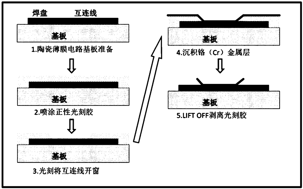
[0042] see image 3 A method for manufacturing a metal solder mask for high-density microwave circuit assembly, comprising the following steps:

[0043] Step 1: Clean the substrate. Clean the surface of the microwave circuit substrate to remove surface dirt.

[0044] Step 2: Spray photoresist. Spray photoresist over the pads and interconnect lines of the substrate.

[0045] Step 3: Open the window by photolithography. Alignment UV lithography was performed, developed to remove the photoresist above the transmission line, and the surface was cleaned by reactive ion etching with oxygen plasma.

[0046] Step 4: Deposit a metal layer. A met...


PUM

PropertyMeasurementUnit
Thicknessaaaaaaaaaa
Thicknessaaaaaaaaaa
Thicknessaaaaaaaaaa

Abstract

Aiming at the problem of a soldering-resistant film between a bonding pad and an interconnection line in assembly of a high-density thin film microwave circuit, the invention provides a fabrication method of a metal soldering-resistant film for assembly of a high-density microwave circuit and a product. The fabrication method comprises the steps of 1, cleaning a substrate; 2, spraying photoresist; 3, photoetching a window; 4, depositing a metal layer; and 5, stripping the photoresist to obtain a Cr soldering-resistant film structure with an edge upwards tiling. The product comprises a microwave circuit substrate, the interconnection line, bonding pads and a Cr metal soldering-resistant film. The fabrication method has the advantages that the process compatibility is high, and a thin film circuit substrate process, namely photoetching and thin film metal deposition, is used; a bonding force with a metal layer on a non-welding region is high, and no extra stress is generated; and the soldering-resistant requirement of a narrow-pitch circuit is met. The edge soldering-resistant film plays a role in improving soldering resistance, and liquid soldering flux is prevented from overflowing out of the interconnection line during the reflow soldering process of a soldering ball.

Description

technical field [0001] The invention belongs to the technical field of microcircuit assembly, and in particular relates to a pretreatment method of a microwave circuit substrate before chip bump bonding, in particular to a method and a product of a metal solder mask for high-density microwave circuit assembly. Background technique [0002] With the development of light weight, thinner, miniaturized, I / O terminals, and functional diversification, traditional packaging technology can no longer meet the high-density requirements. New microelectronic packaging technologies that have developed rapidly since the 1990s, including ball array packaging (BGA), chip scale packaging (CSP), wafer level packaging (WLP), three-dimensional packaging (3D) and system in package (SIP) and other technologies have greatly promoted the development of high-density packaging. At the same time, high density, fine circuits and narrow pitch put forward higher requirements for microcircuit assembly. I...

Claims


Application Information

Patent Timeline
IPC IPC(8): H01L21/48
CPCH01L21/4846
Inventor 郭育华宋夏陈帅魏晓旻邱颖霞
Owner CHINA ELECTRONIC TECH GRP CORP NO 38 RES INST
Features
  • R&D
  • Intellectual Property
  • Life Sciences
  • Materials
  • Tech Scout
  • Unparalleled Data Quality
  • Higher Quality Content
  • 60% Fewer Hallucinations
Learn More