A kind of ge-se-zn chalcogenide film material for optical waveguide and preparation method thereof

A ge-se-zn, chalcogenide thin film technology, applied in the field of optoelectronics, can solve the problems of easy devitrification of deposited thin films, easy photo-induced changes, poor stability, etc.

Active Publication Date: 2019-06-18
NINGBO UNIV
View PDF2 Cites 0 Cited by
  • Summary
  • Abstract
  • Description
  • Claims
  • Application Information

AI Technical Summary

Problems solved by technology

ZnSe chalcogenide thin film has excellent optical properties, and because of its unique structural characteristics that are extremely sensitive to light response, it is easy to undergo photoinduced changes, and has good application prospects in optical storage and other optical fields. However, the as-deposited thin film Easy to crystallize, poor stability

Method used


Image

  • A kind of ge-se-zn chalcogenide film material for optical waveguide and preparation method thereof
  • A kind of ge-se-zn chalcogenide film material for optical waveguide and preparation method thereof
  • A kind of ge-se-zn chalcogenide film material for optical waveguide and preparation method thereof

Examples


Embodiment 1

[0023] The present invention is a kind of Ge-Se-Zn chalcogenide film material used for optical waveguide, its chemical structure formula is Zn x Se y Ge z , wherein 28

[0024] In the magnetron sputtering coating system, the quartz sheet or silicon oxide sheet is used as the substrate, the ZnSe alloy target is installed in the magnetron radio frequency sputtering target, and the Ge target is installed in the magnetron DC sputtering target. The sputtering chamber of the magnetron sputtering coating system was evacuated until the vacuum degree in the chamber reached 2.4×10 -4 Pa, then feed into the sputtering chamber a high-purity argon with a volume flow rate of 50ml / min until the air pressure in the sputtering chamber reaches the required initiation pressure of 0.25Pa for sputtering, and then control the sputtering power of the ZnSe alloy target to be 70W, The sputtering power of the Ge singl...

Embodiment 2

[0027] It is basically the same as Example 1, the difference is that in the sputtering process, the sputtering power of the alloy ZnSe target is controlled to be 70W, the sputtering power of the Ge simple substance target is 8W, and the film thickness is controlled at 1µm, and the obtained Zn x Se y Ge z Thin film, where x=35.1, y=39, z=25.9, namely Zn 35.1 Se 39 Ge 25.9 .

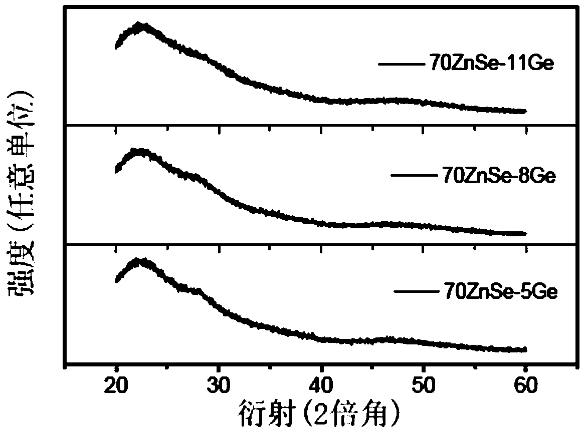
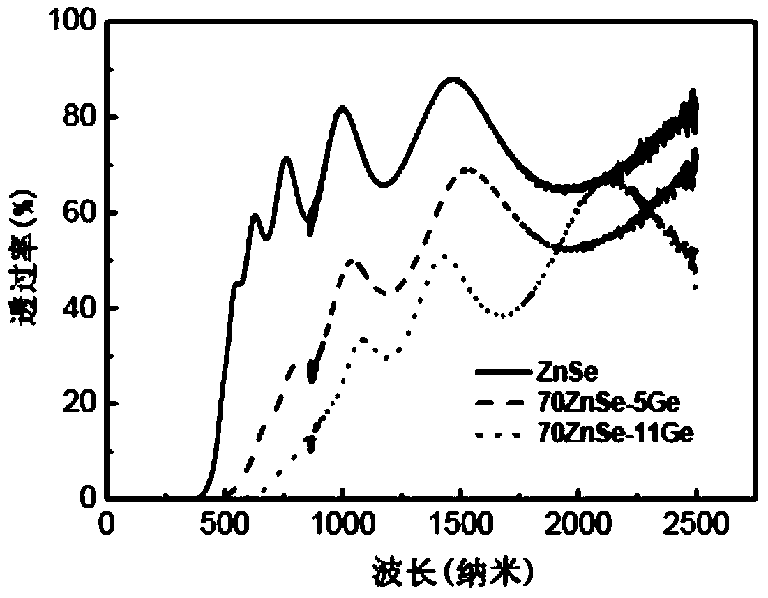
[0028] The prepared film was subjected to XRD and AFM performance tests, and the test results were as follows figure 2 and Table 1, from figure 2 It can be seen from Table 1 that the performance indicators of the film prepared in Example 2 are as follows; the deposited film is amorphous, the roughness is 1.745, the transmittance is 50%, and the short-wave cut-off edge is 850nm.

Embodiment 3

[0030] It is basically the same as Example 1, the difference is that in the sputtering process, the sputtering power of the alloy ZnSe target is controlled to be 70W, the sputtering power of the Ge simple substance target is 11W, and the film thickness is controlled at 1 μm, and the obtained Zn x Se y Ge z Film, where x=33.4, y=35.1, z=31.5, namely Zn 33.4 Sb 35.1 Te 31.5 .

[0031] The prepared film was subjected to XRD and AFM performance tests, and the test results were as follows figure 2 and Table 1, from figure 2It can be seen from Table 1 that the performance indicators of the thin film prepared in Example 3 are as follows: the deposited thin film is amorphous, the roughness is 1.214nm, the transmittance is 40%, and the short-wave cut-off edge is 1000nm.


PUM

PropertyMeasurementUnit
surface roughnessaaaaaaaaaa

Abstract

The invention discloses a Zn-Se-Ge sulfur-based thin film material for optical waveguide, and a preparation method thereof. The Zn-Se-Ge sulfur-based thin film material is characterized in that the chemical structure formula is ZnxSeyGez, wherein x is more than 28 and is less than 40, y is more than 30 and is less than 45, z is more than 15 and is less than 40, and the sum of x, y and z is 100. The preparation method comprises: arranging a ZnSe alloy target material in a magnetron radio frequency sputtering target, arranging a Ge elementary target material in a magnetron direct current target, vacuumizing the sputtering chamber of a magnetron sputtering film plating system to achieve an inside-chamber vacuum degree of 2.5*10<4> Pa, introducing high-purity argon at a speed of 50 ml / min until the start-up pressure achieves 0.25 Pa, controlling the sputtering power of the Ge target at 0-11 W, fixing the sputtering power of the ZnSe alloy target at 70 W, and carrying out sputtering film plating at a room temperature. The prepared Zn-Se-Ge sulfur-based thin film material of the present invention has advantages of high stability, low roughness, high transmittance, short short-wave cutoff edge, low thin film component deviation, and stable structure.

Description

technical field [0001] The invention relates to the field of optoelectronics, in particular to a Ge-Se-Zn chalcogenide thin film used for an optical waveguide and a preparation method thereof. Background technique [0002] Chalcogenide glasses, due to their structural flexibility (low coordination of chalcogen elements and the existence of lone pairs of electrons at the highest point in the valence band), exhibit many photoinduced changes under near-bandgap illumination, which cause changes in electronic and atomic structures. , phase, physical and chemical properties and other changes. For example, under laser induction, the short-wave absorption cut-off edge of the deposited chalcogenide film may be red-shifted to the long-wave direction (that is, photo-induced darkening), or blue-shifted to the short-wave direction (that is, photo-induced darkening). bleaching) and cause changes in the refractive index. Illumination may also cause changes in volume (such as photo-induce...

Claims


Application Information

Patent Timeline
Patent Type & Authority Patents(China)
IPC IPC(8): C23C14/35C23C14/06
CPCC23C14/06C23C14/352
Inventor 王慧王国祥沈祥许银生陈飞飞吕业刚聂秋华焦清师道田陈益敏
Owner NINGBO UNIV
Why Eureka
Try Eureka