A silicon-based apd integrated circuit

An integrated circuit, silicon-based technology, applied in circuits, electrical components, electrical solid devices, etc., can solve the problems of light-current gain and response speed gap, poor isolation effect, easy to produce parasitic effects, etc., to achieve fast response speed, The effect of low power consumption, reduced packaging difficulty and parasitic effects

Active Publication Date: 2019-02-05
南京紫科光电科技有限公司
View PDF6 Cites 0 Cited by
  • Summary
  • Abstract
  • Description
  • Claims
  • Application Information

AI Technical Summary

Problems solved by technology

However, its structure is an improvement of the traditional structure, and its photo-current gain and response speed still have a certain gap compared with the avalanche breakdown diode.
[0007] Another example is that a photodetector used in a silicon-based optoelectronic integrated circuit chip involved in Chinese Patent Publication No. CN103872168A adopts a lateral structure. However, compared with the V-shaped groove structure in this patent, its isolation effect from other components Poor, prone to parasitic effects

Method used


Image

  • A silicon-based apd integrated circuit
  • A silicon-based apd integrated circuit
  • A silicon-based apd integrated circuit

Examples


Embodiment Construction

[0032] In order to make the technical means, creative features, goals and effects achieved by the present invention easy to understand, the present invention will be further described below in conjunction with specific illustrations.

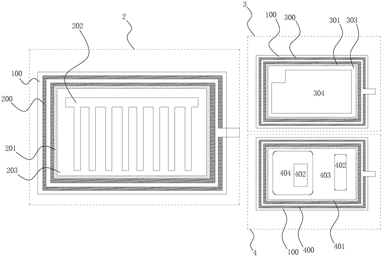
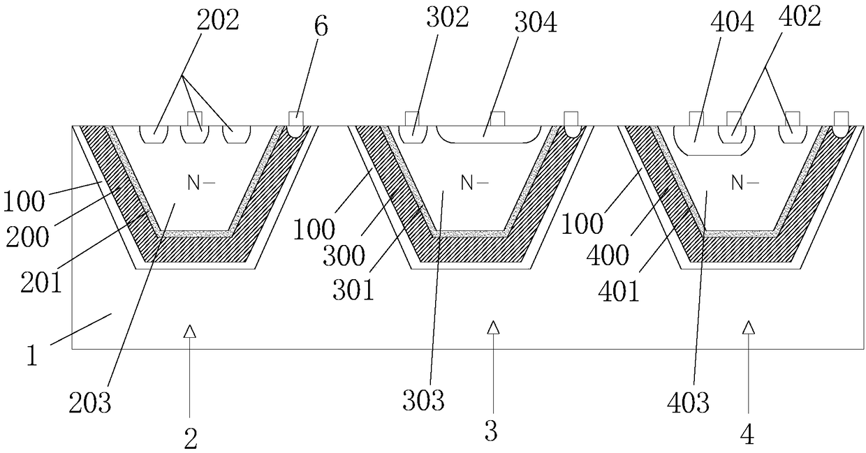
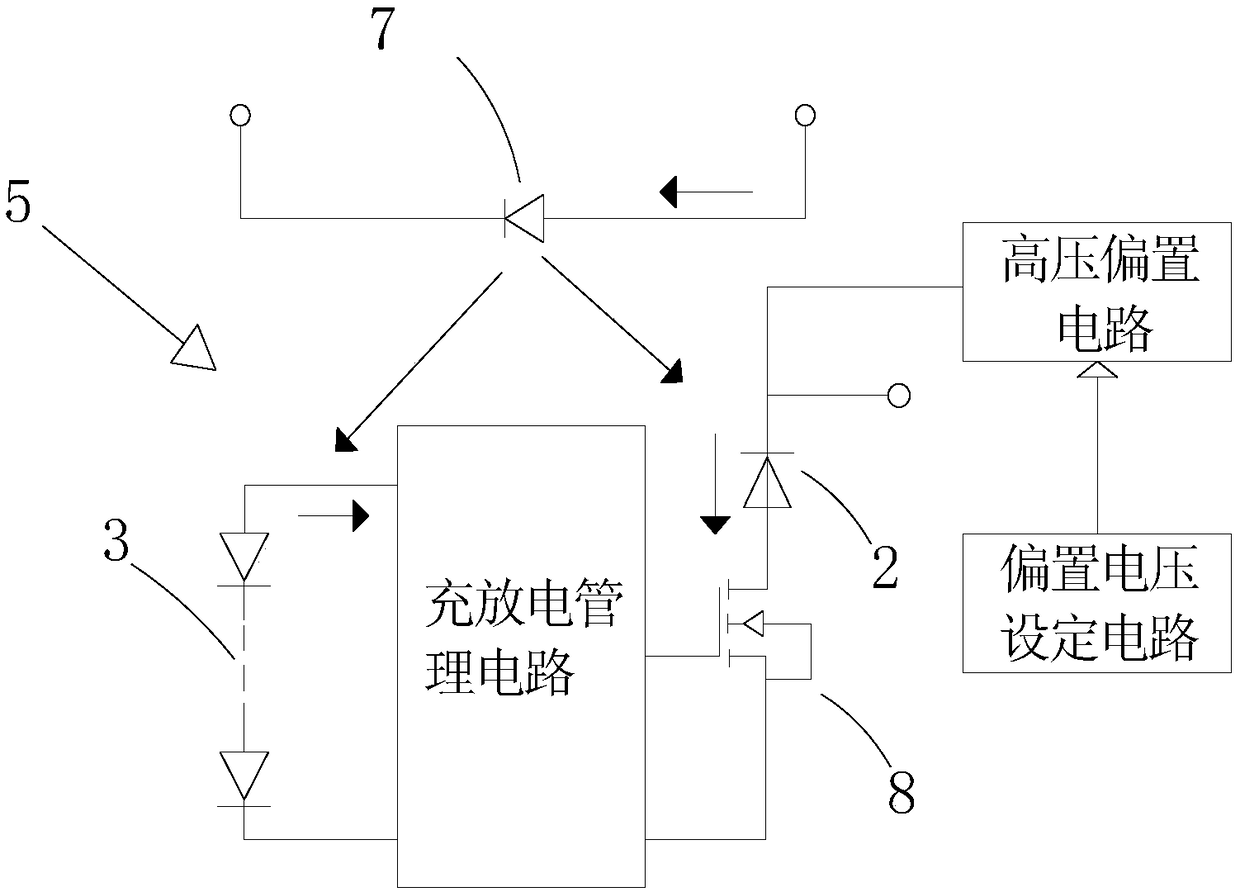
[0033] Such as Figure 1-3 Shown, a kind of integrated circuit of silicon-based APD, it comprises substrate 1, silicon-based avalanche photodiode 2, photovoltaic diode array 3, bipolar NPN triode 4 and other management circuit 5 (such as image 3 As shown), the substrate 1 is provided with an array of V-shaped grooves 100, and the silicon-based avalanche photodiode 2, photovoltaic diode array 3 and bipolar NPN triode 4 are respectively arranged in a V-shaped groove 100 , and integrated with the management circuit 5 on the same substrate 1 . The substrate 1 is made of polysilicon material.

[0034] Such as figure 2 As shown, the V-shaped groove 100 provided with the silicon-based avalanche photodiode 2 has a low-doped P layer 200, a highly do...


PUM


Abstract

The invention discloses a silicon-based APD integrated circuit, which belongs to the technical field of optoelectronic integration. The silicon-based APD integrated circuit comprises a substrate, a silicon-based avalanche photodiode (APD), a photovoltaic diode array, a bipolar NPN transistor and a management circuit formed by resistors and capacitors, wherein a plurality of groups of V-type grooves are arranged in the substrate; the silicon-based avalanche photodiode, the photovoltaic diode array and the bipolar NPN transistor are arranged in one V-type groove and are integrated on the same substrate with the management circuit. The integrated circuit combines the traditional V-type groove process and the bipolar process, the structure is simple, the reliability is high, the crosstalk is little, and the power consumption is low.

Description

technical field [0001] The invention relates to the technical field of optoelectronic integration, in particular to an integrated circuit for driving silicon-based avalanche photodiodes. Background technique [0002] An optoelectronic integrated circuit refers to an integrated circuit that integrates optoelectronic devices and microelectronic devices on the same substrate to achieve a specific function. It greatly eliminates the negative parasitic effects in traditional circuits and reduces hybrid circuits. In the assembly link, the electrical signal output by the electronic device is converted into an optical signal with excellent multiplexing ability, lower transmission loss, stronger anti-interference performance and better transmission speed, because these remarkable characteristics are widely used in Optical fiber communication, optical control radar system, optical disc system, medical system, laser ranging and photoelectric detection and other fields. Silicon-based o...

Claims


Application Information

Patent Timeline
Patent Type & Authority Patents(China)
IPC IPC(8): H01L27/144
CPCH01L27/144H01L27/1443
Inventor 谢峰吴浩然周东陆海
Owner 南京紫科光电科技有限公司
Why Eureka
Try Eureka