Frequency reconfigurable coupled feed loop antenna

A loop antenna, coupled feed technology, applied to loop antennas, antennas, antenna parts and other directions, can solve the problem of increasing the difficulty of antenna design, and achieve the effects of simple structure, low profile and small volume

Inactive Publication Date: 2017-04-26
XIAN CREATION KEJI CO LTD
View PDF0 Cites 5 Cited by
  • Summary
  • Abstract
  • Description
  • Claims
  • Application Information

AI Technical Summary

Problems solved by technology

Since the design of the reconfigurable antenna needs to consider the mutual coupling b

Method used


Image

  • Frequency reconfigurable coupled feed loop antenna
  • Frequency reconfigurable coupled feed loop antenna
  • Frequency reconfigurable coupled feed loop antenna

Examples


Embodiment 1

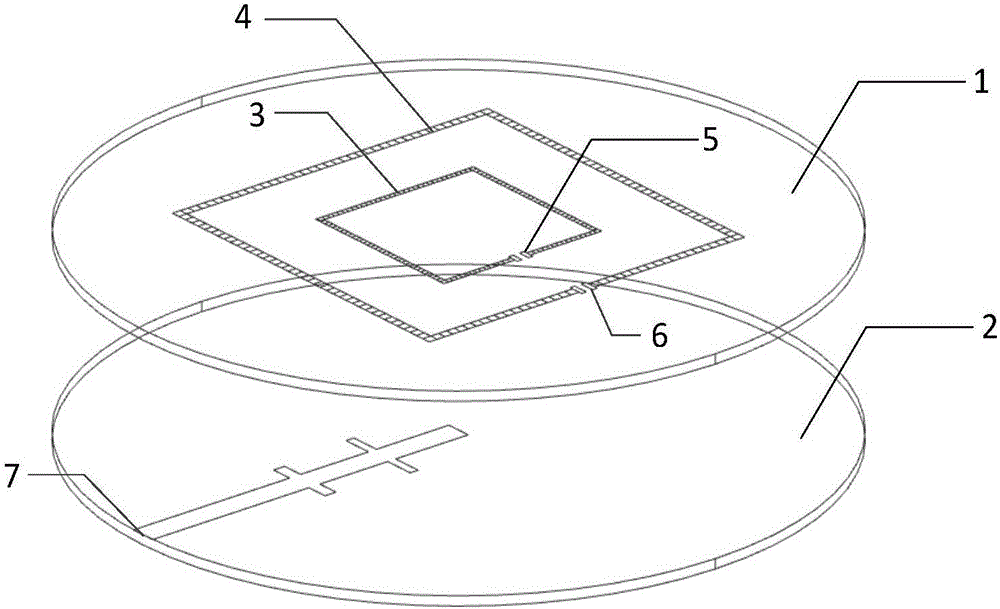
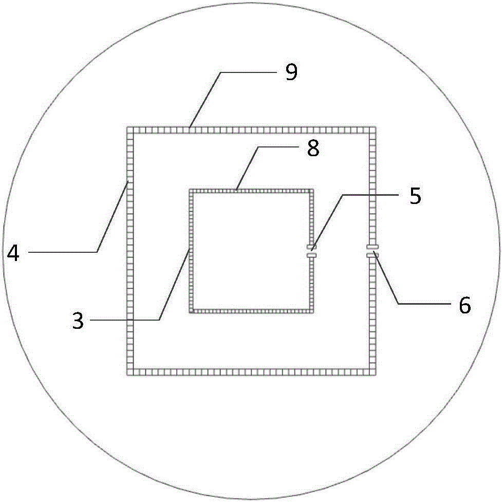
[0030] See figure 2 , figure 2 It is a structural schematic diagram of an SOI fundamental frequency reconfigurable coupled feeding loop antenna based on SPiN diodes provided by an embodiment of the present invention. The frequency reconfigurable coupling feed loop antenna includes a semiconductor substrate 1, a dielectric plate 2, a first SPiN diode ring 3, a second SPiN diode ring 4, a first DC bias line 5, and a second DC bias line 6 , are all arranged on the semiconductor substrate 1 ; the coupled feed 7 is arranged on the dielectric board 2 .

[0031] The above-mentioned frequency reconfigurable coupling feeding loop antenna, the first SPiN diode ring 3, the second SPiN diode ring 4, the first DC bias line 5 and the second DC bias line 6 adopt A semiconductor process is fabricated on the semiconductor substrate 1 .

[0032] The above-mentioned frequency reconfigurable coupling feeding loop antenna, the semiconductor substrate 1 and the dielectric plate 2 are Si-based ...

Embodiment 2

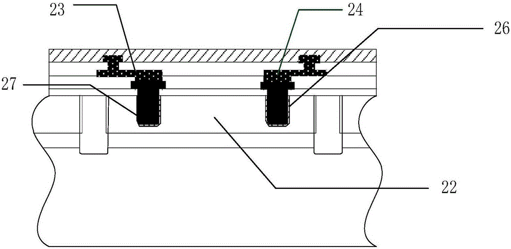
[0042] Please also see figure 1 and Figure 5 , figure 1 It is a schematic diagram of the SPiN diode structure provided by the embodiment of the present invention, Figure 5It is a schematic structural diagram of an SPiN diode string provided by an embodiment of the present invention. Each SPiN diode string includes a plurality of SPiN diodes, and these SPiN diodes are connected in series. The SPiN diode is composed of a P+ region 27, an N+ region 26 and an intrinsic region 22, the first metal contact region 23 is located at the P+ region 27, the second metal contact region 24 is located at the N+ region 26, and the SPiN at one end of the SPiN diode string The metal contact region 23 of the diode is connected to the anode of the DC bias, and the metal contact region 24 of the SPiN diode at the other end of the SPiN diode string can make all the SPiN diodes in the entire SPiN diode string in a forward conduction state by applying a DC voltage. When using SPiN diode forward ...


PUM


Abstract

The invention belongs to the solid-state plasma and microstrip antenna technology, and more particularly, to a frequency reconfigurable coupled feed loop antenna, comprising: a semiconductor substrate, a dielectic plate, SPiN diode rings, a DC bias line, and a coupling feed source. When a metal contact area is connected to the positive electrode and the negative electrode of the DC bias line respectively, through the exerted DC current and voltage, all SPiN diode rings in the entire SPiN diode string can be put into a forward communication state. When the SPiN diodes are used to excite the solid-state plasma in forward-bias manner, the diodes can be applied for the electromagnetic radiation of the antenna. When the SPiN diodes are closed without bias, they take on a semiconductor dielectric state which can solve the mutually coupling problem between antennas so as to facilitate the design of a reconfigurable antenna. The frequency reconfigurable coupled feed loop antenna of the invention is small in size, reconfigurable, easy to be integrated, and has a simple structure. With the antenna, feeding becomes easy; and frequency can be jumped rapidly.

Description

technical field [0001] The invention belongs to the technical field of solid-state plasma and microstrip antenna, and in particular relates to a frequency reconfigurable coupling feeding loop antenna. Background technique [0002] With the further development of science and technology, wireless communication technology is playing an increasingly important role in people's lives. The development trend of the new-generation wireless communication system includes realizing high-speed data transmission, realizing the interconnection between multiple wireless systems, realizing the effective use of limited spectrum resources, and obtaining the ability to adapt to the surrounding environment, etc. Therefore, the requirements for antennas in the communication field are getting higher and higher. [0003] The antennas that have been researched so far are basically made of metal, so the shape of this antenna cannot be changed after it is manufactured, and it has a large radar scatte...

Claims


Application Information

Patent Timeline
IPC IPC(8): H01Q1/22H01Q1/36H01Q1/50H01Q7/00H01Q5/321
CPCH01Q1/2283H01Q1/36H01Q1/50H01Q5/321H01Q7/00
Inventor 王起舒圣杰
Owner XIAN CREATION KEJI CO LTD
Why Eureka
Try Eureka