
Semiconductor-based, large-area, flexible electronic devices on {110}<100> oriented substrates

A technology of electronic devices and semiconductors, applied in the direction of semiconductor devices, semiconductor/solid-state device manufacturing, electrical components, etc.

Inactive Publication Date: 2017-05-10
阿米特·戈亚尔
View PDF22 Cites 2 Cited by
  • Summary
  • Abstract
  • Description
  • Claims
  • Application Information

AI Technical Summary

Problems solved by technology

Also, for some applications semiconductor surfaces / films / wafers need to be flexible, enabling applications where curved semiconductors may be desirable

Method used


Image

  • Semiconductor-based, large-area, flexible electronic devices on {110}&lt;100&gt; oriented substrates
  • Semiconductor-based, large-area, flexible electronic devices on {110}&lt;100&gt; oriented substrates
  • Semiconductor-based, large-area, flexible electronic devices on {110}&lt;100&gt; oriented substrates

Examples


Embodiment 1

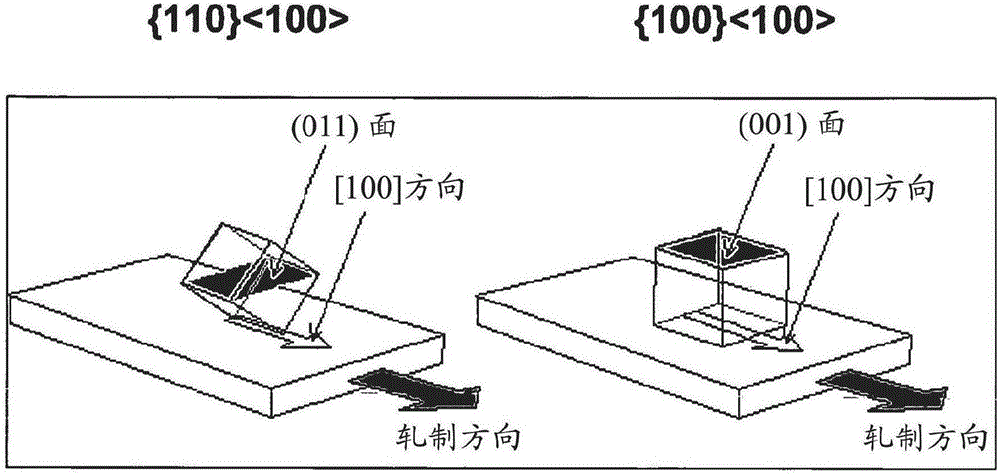
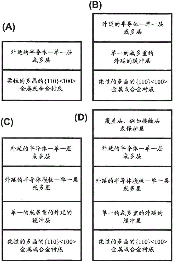
[0096] Example 1: [100] uniaxially textured metal substrates were prepared by successively pressing or forging cubic metals or alloys by compression to a large total deformation and then recrystallization annealing. For example, a NiW alloy with 3-9 at% W is used, compressed to 90% deformation by uniaxial extrusion, and then annealed in a furnace at a temperature above the primary recrystallization temperature of the alloy. The primary recrystallized texture formed is the [100] texture. By increasing the annealing temperature to a high temperature close to 1000°C, an average grain size of greater than 100 μm is formed. An epitaxial buffer layer is then deposited on the substrate. For example, chemical vapor deposition (CVD) is used to deposit epitaxial TiN layers at deposition temperatures ranging from 300°C to 600°C. An epitaxial Si layer is then deposited using a CVD type process at a deposition temperature ranging from 300°C to 900°C. This results in the formation of a [...

Embodiment 2

[0097] Example 2: [110] uniaxially textured metal substrates were prepared by successively pressing cubic metals or alloys by compression to a large total deformation and then recrystallization annealing. For example, a NiW alloy with 3-9 at% W is used, compressed to 90% deformation by uniaxial extrusion, and then annealed in a furnace at a temperature above the primary recrystallization temperature of the alloy. The primary recrystallized texture formed is the [110] texture. By increasing the annealing temperature to a high temperature close to 1000°C, an average grain size of greater than 100 μm is formed. An epitaxial buffer layer is then deposited on the substrate. For example, chemical vapor deposition (CVD) is used to deposit epitaxial TiN layers at deposition temperatures ranging from 300°C to 600°C. An epitaxial Si layer is then deposited using a CVD type process at a deposition temperature ranging from 300°C to 900°C. This results in the formation of a [110] uniaxi...

Embodiment 3

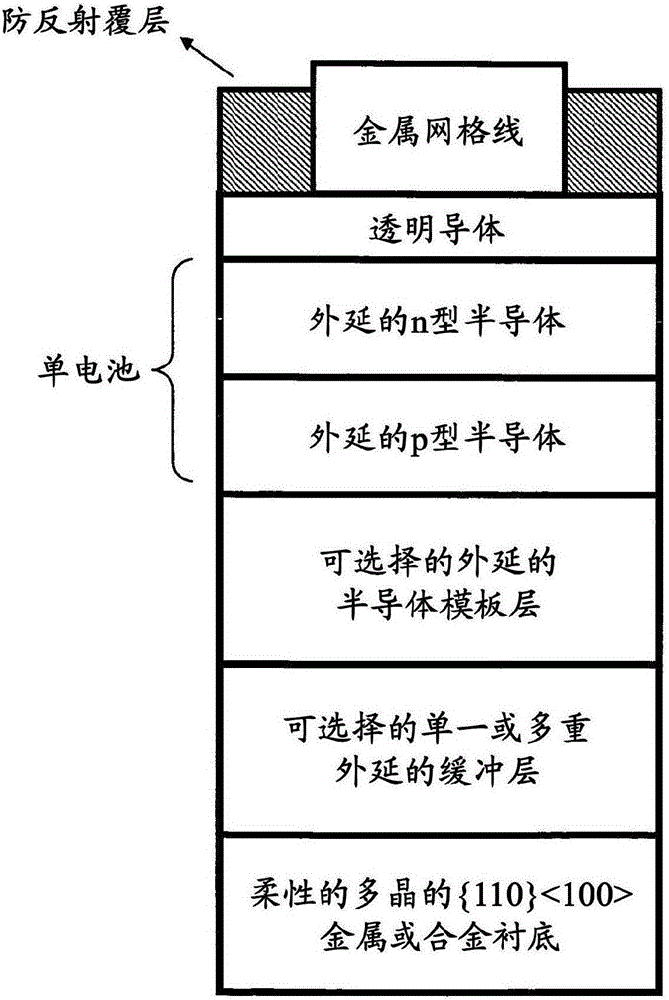
[0098] Example 3: Figure 10 Shown in cross-section of a crystallographically textured, flexible NiW alloy with a textured Si semiconductor layer over the alloy and an epitaxial buffer layer of textured TiN in between idealized schematic diagram. [100] textured biaxially textured Ni-3at%W was prepared by continuous rolling of powder metallurgy obtained alloy coils from a thickness of about 120 mils to a foil thickness of about 2 mils or 50 microns. The rolled crystallographic texture of the foil or strip is the standard Cu-type rolled texture of greatly deformed FCC metals. After degreasing and drying the tape, the tape was loaded into a reel-to-reel high vacuum (10-8 Torr) chamber containing a radio frequency induction furnace. The strip was pulled through the hot zone of the furnace under a partial pressure of ~3 x 10⁻⁷ Torr of hydrogen sulfide gas at a rate such that each section was heated to 1250° C. in twenty minutes, so as to be on the surface of the strip. A sulfur ...


PUM

PropertyMeasurementUnit
crystal sizeaaaaaaaaaa
diameteraaaaaaaaaa
areaaaaaaaaaaa

Abstract

The invention relates to semiconductor-based, large-area, flexible electronic devices on {110}<100> oriented substrates. Novel articles and methods to fabricate the same resulting in flexible, {110}<100> or 45-degree-rotated {110}<100> oriented, semiconductor-based electronic devices are disclosed. Potential applications of resulting articles are in areas of photovoltaic devices, flat-panel displays, thermophotovoltaic devices, ferroelectric devices, light emitting diode devices,, computer hard disc drive devices, magnetoresistance based devices, photoluminescence based devices, non-volatile memory devices, dielectric devices, thermoelectric devices and quantum dot laser devices.

Description

[0001] This application is filed on September 9, 2008, the application number is "200880129020.1", and the title of the invention is "Semiconductor-based large-area flexible electronic device on a {110}<100>-oriented substrate" Divisional application. [0002] Statement Regarding Federally Sponsored Research or Development [0003] This invention was made with Government support under Contract No. DE-AC05-000R22725 awarded by the US Department of Energy. The government has certain rights in this invention. [0004] field of invention [0005] The present invention relates to the fabrication of high performance electronic devices including various types of semiconductors and articles derived therefrom. [0006] Background of the invention [0007] This international application is the PCT application corresponding to US Patent Application Serial No. 12 / 079,068, filed March 25, 2008. US Patent Application Serial No. 12 / 079,068 is a continuation-in-part of US Patent Appl...

Claims


Application Information

Patent Timeline
Patent Type & Authority Applications(China)
IPC IPC(8): H01L29/04H01L29/12H01L29/20H01L31/0392H01L21/02B82Y10/00
CPCB82Y10/00H01L21/0237H01L21/0242H01L21/02425H01L21/02428H01L21/02433H01L21/02491H01L21/02502H01L21/02516H01L21/02521H01L21/02532H01L21/02538H01L29/045H01L29/127H01L29/2003H01L31/0392H01L31/03923H01L31/03925Y02E10/541
Inventor 阿米特·戈亚尔
Owner 阿米特·戈亚尔
Learn More