A kind of LED chip and its manufacturing method

A technology of LED chip and manufacturing method, which is applied in the direction of semiconductor devices, electrical components, circuits, etc., can solve the problems of easily damaged structure, poor effect of improving LED luminous efficiency, and not tightly bonded ZnO seeds, etc., so as to improve the current expansion ability , reduced light absorption, effects of high carrier concentration and mobility

Active Publication Date: 2019-06-11
HC SEMITEK ZHEJIANG CO LTD
View PDF5 Cites 0 Cited by
  • Summary
  • Abstract
  • Description
  • Claims
  • Application Information

AI Technical Summary

Problems solved by technology

[0005] The ZnO seeds produced by the precipitation method are not tightly bonded, the structure is easily destroyed, and the improvement effect of LED luminous efficiency is poor

Method used


Image

  • A kind of LED chip and its manufacturing method
  • A kind of LED chip and its manufacturing method

Examples


Embodiment 1

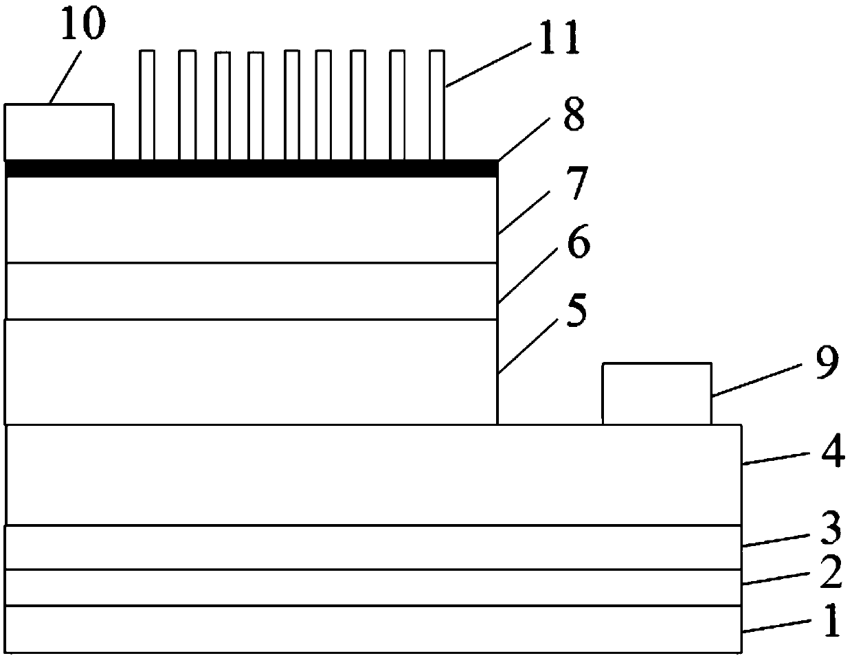
[0042] An embodiment of the present invention provides an LED chip, see figure 1 , the LED chip includes a substrate 1, and an undoped AlN buffer layer 2, an undoped GaN layer 3, an N-type GaN layer 4, a multi-quantum well layer 5, a P-type Al y Ga 1-y N layer 6, P-type GaN layer 7, graphene thin film layer 8, 0.1

[0043] In this embodiment, the LED chip also includes several TiO 2 nanorods 11, some TiO 2 The nanorods 11 are arranged on the graphene film layer 8 in an array.

[0044] Optionally, TiO 2 The diameter of the nanorods may be 20-80 nm.

[0045] Optionally, TiO 2 The height of the nanorods can be 300-500 nm.

[0046] Optionally, TiO...

Embodiment 2

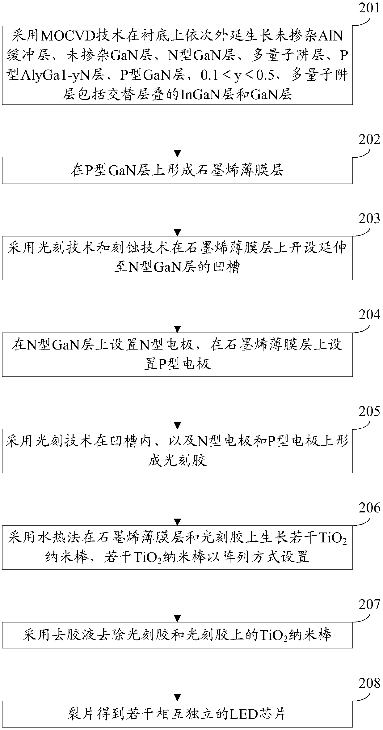
[0050] The embodiment of the present invention provides a method for manufacturing an LED chip, which is suitable for manufacturing the LED chip provided in Embodiment 1, see figure 2 , the production method includes:

[0051] Step 201: Epitaxially grow an undoped AlN buffer layer, an undoped GaN layer, an N-type GaN layer, a multi-quantum Well layer, P-type AlyGa1-yN layer, P-type GaN layer, 0.1

[0052] Optionally, the substrate may be a GaAs substrate suitable for red and yellow LEDs, or a sapphire substrate, SiC substrate or GaN substrate suitable for blue and green LEDs.

[0053] Step 202: forming a graphene film layer on the p-type GaN layer.

[0054] Specifically, this step 202 may include:

[0055] Using chemical vapor deposition technology (English: Chemical Vapor Deposition), referred to as: CVD) to prepare graphene films on nickel metal substrates;

[0056] Coating the first...


PUM


Abstract

The invention discloses an LED chip and a preparation method thereof, and belongs to the technical field of semiconductors. The LED chip comprises a substrate, an undoped AlN buffer layer, an undoped GaN layer, an N-type GaN layer, a multi-quantum well layer, a P-type Al<y>Ga<1-y>N layer, a P-type GaN layer and a graphene film layer, wherein the undoped AlN buffer layer, the undoped GaN layer, the N-type GaN layer, the multi-quantum well layer, the P-type Al<y>Ga<1-y>N layer, the P-type GaN layer and the graphene film layer are sequentially stacked on the substrate; y is smaller than 0.5 and greater than 0.1; the multi-quantum well layer comprises an InGaN layer and a GaN layer which are alternately stacked; a groove which extends to the N-type GaN layer is formed in the graphene film layer; an N-type electrode is arranged on the N-type GaN layer; a P-type electrode is arranged on the graphene film layer; and multiple TiO2 nanorods are arranged on the graphene film layer in an array manner. The graphene film layer can be directly adopted as a seed layer through formation of the TiO2 nanorods, and the seed layer is tightly combined and is not easily destroyed, so that the light-emitting efficiency of an LED can be obviously improved.

Description

technical field [0001] The invention relates to the technical field of semiconductors, in particular to an LED chip and a manufacturing method thereof. Background technique [0002] With the development of semiconductor technology, the luminous efficiency of light-emitting diodes (English: Light Emitting Diode, referred to as: LED) has been continuously improved, and it has been widely used in various color display screens, decorative lights, indicator lights, white light lighting, etc. But the luminous efficiency of LED has not yet reached the ideal goal. [0003] The luminous efficiency of LED is determined by two aspects: internal quantum efficiency and light extraction efficiency. The internal quantum efficiency of existing blue GaN-based LEDs is already very high, mainly to improve the light extraction efficiency of LEDs. At present, a layer of ZnO seed layer is fabricated on the current spreading layer of LED by precipitation method, and ZnO nanorod array is grown by ...

Claims


Application Information

Patent Timeline
Patent Type & Authority Patents(China)
IPC IPC(8): H01L33/44H01L33/42H01L33/00
CPCH01L33/0075H01L33/42H01L33/44
Inventor 丁涛郭炳磊葛永晖吕蒙普胡加辉李鹏
Owner HC SEMITEK ZHEJIANG CO LTD
Why Eureka
Try Eureka