A p-gan/i-gan/n-bn neutron detector

A neutron detector and p-gan technology, applied in the field of nuclear radiation detection, can solve the problems of neutron conversion layer and low detection efficiency, and achieve the effects of low cost, improved detection efficiency and excellent performance

Active Publication Date: 2018-08-28
EAST CHINA UNIV OF TECH
View PDF4 Cites 1 Cited by
  • Summary
  • Abstract
  • Description
  • Claims
  • Application Information

AI Technical Summary

Problems solved by technology

[0003] The object of the present invention aims at the deficiencies of existing neutron detectors that require neutron conversion layers and low detection efficiency. The present invention provides a p-GaN / i-GaN / n-BN neutron detector and its preparation method

Method used


Image

  • A p-gan/i-gan/n-bn neutron detector
  • A p-gan/i-gan/n-bn neutron detector
  • A p-gan/i-gan/n-bn neutron detector

Examples


Embodiment 1

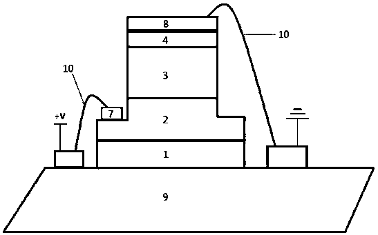
[0032] The p-GaN / i-GaN / n-BN neutron detector of the present invention and its preparation method, the detector is suitable for detecting low-energy thermal neutrons:

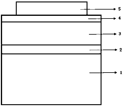
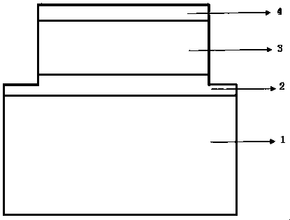
[0033] First, 150 μm thick Al 2 o 3 The substrate 1 is placed in the growth chamber of the metal-organic chemical vapor deposition equipment, and then the Al 2 o 3 The substrate 1 is heated to 1100° C. and baked at high temperature for 10 minutes to remove impurities on the surface of the substrate. First grow a GaN buffer layer with a thickness of 20nm at 550°C, then raise the temperature to 1350°C to grow n-BN thin film 2, hydrogen sulfide is used as the gas doping source, and the doping concentration is 5×10 18 cm -3 , with a thickness of 20 μm; again at a temperature of 1050 ° C, epitaxially grow an undoped i-GaN film 3 on the n-BN film 2 with a thickness of 10 μm; finally at a temperature of 950 ° C, on the n-GaN / i -GaN film epitaxial growth p-GaN film 4 ( figure 2 ), magnesium dicene as the gas dopi...

Embodiment 2

[0039] The preparation method of the neutron detector with p-GaN / i-GaN / n-BN structure of the present invention, the detector is suitable for detecting fast neutrons with an energy of 0.1-5 MeV, and a polyethylene switch is placed between the neutron source and the detector agent:

[0040] First, a 200 μm thick Al 2 o 3 The substrate 1 is placed in the growth chamber of the metal-organic chemical vapor deposition equipment, and then the Al 2 o 3 The substrate 1 is heated to 1100° C. and baked at high temperature for 10 minutes to remove impurities on the surface of the substrate. First grow a GaN buffer layer with a thickness of 20nm at 550°C, then raise the temperature to 1400°C to grow n-BN film 2, hydrogen sulfide is used as the gas doping source, and the doping concentration is 6×10 18 cm -3 , with a thickness of 30 μm; again at a temperature of 1050 ° C, epitaxially grow an undoped i-GaN film 3 on the n-BN film 2 with a thickness of 15 μm; finally at a temperature of ...

Embodiment 3

[0046] The preparation method of the neutron detector with p-GaN / i-GaN / n-BN structure of the present invention, the detector is suitable for detecting fast neutrons with an energy of 0.1-10 MeV, and a polyethylene switch is placed between the neutron source and the detector agent:

[0047] First, 150 μm thick Al 2 o 3 The substrate 1 is placed in the growth chamber of the metal-organic chemical vapor deposition equipment, and then the Al 2 o 3The substrate 1 is heated to 1100° C. and baked at high temperature for 10 minutes to remove impurities on the surface of the substrate. First grow a GaN buffer layer with a thickness of 20nm at 550°C, and then raise the temperature to 1500°C to grow n-BN thin film 2, hydrogen sulfide is used as the gas doping source, and the doping concentration is 8×10 18 cm -3 , with a thickness of 50 μm; again at a temperature of 1050 ° C, epitaxially grow an undoped i-GaN film 3 on the n-BN film 2 with a thickness of 20 μm; finally at a temperat...


PUM


Abstract

The invention discloses a p-GaN / i-GaN / n-BN neutron detector. The neutron detector is composed of an Al2O3 substrate layer, an n-BN layer, an i-GaN layer and a p-GaN layer. The preparation method is as follows: on an Al2O3 substrate with a certain thickness, firstly grow n-BN by using metal organic chemical vapor deposition technology, then grow undoped i-GaN, and finally grow p-GaN, and then use inductively coupled plasma etching. The n-BN is etched out, and finally ohmic contact metal electrodes are evaporated on the n-BN and p-GaN layers by electron beam evaporation to complete the fabrication of the neutron detector. The invention has simple preparation process, does not need to prepare a neutron conversion layer separately, has high energy resolution, high detection efficiency and simple structure, and has important application value in aerospace exploration, nuclear energy utilization and development, generation and application of radioisotopes and some special fields .

Description

technical field [0001] The invention relates to the technical field of nuclear radiation detection, in particular to a p-GaN / i-GaN / n-BN neutron detector. Background technique [0002] The neutron itself is not charged, and cannot cause ionization and excitation through ionization loss to lose energy. Therefore, a conventional semiconductor neutron detector is deposited on its surface with a certain thickness of neutron conversion layer 6 LiF or B 4 c. The existence of the neutron conversion layer makes the detection efficiency and energy resolution of semiconductor neutron detectors very low. Due to this factor, the further development of semiconductor neutron detectors has been limited to a certain extent in recent years. BN is an important III-V compound wide bandgap semiconductor material with a bandgap width of 6.5eV at room temperature. BN is a neutron detection material that directly detects neutrons and has great potential. 10 B atoms have a high thermal neutron...

Claims


Application Information

Patent Timeline
Patent Type & Authority Patents(China)
IPC IPC(8): H01L31/0304H01L31/117H01L31/18H01L21/02
CPCH01L21/0242H01L21/0254H01L21/0262H01L31/03044H01L31/117H01L31/1852H01L31/1856Y02P70/50
Inventor 朱志甫汤彬邹继军彭新村
Owner EAST CHINA UNIV OF TECH
Why Eureka
Try Eureka