Manufacturing method of ltps array substrate

A manufacturing method and array substrate technology, which are applied in photolithography process exposure devices, semiconductor/solid-state device manufacturing, microlithography exposure equipment, etc. The problem of high cost can reduce the displacement error, reduce the number of masks, and reduce the production cost.

Active Publication Date: 2019-07-02
WUHAN CHINA STAR OPTOELECTRONICS TECH CO LTD
View PDF4 Cites 0 Cited by
  • Summary
  • Abstract
  • Description
  • Claims
  • Application Information

AI Technical Summary

Problems solved by technology

[0006] In the manufacture of the current LTPS array substrate, the manufacturing process of the film structure of the light-shielding layer and the active layer is as follows: first, the glass substrate is cleaned, and the physical vapor deposition method (Physical Vapor Deposition, PVD) is used on the glass substrate. A metal layer is formed, and a photolithography process is used to pattern the metal layer to obtain a light-shielding layer; then a buffer layer is formed on the light-shielding layer and the glass substrate; and then a chemical vapor deposition method (Chemical Vapor Deposition, CVD) forming an amorphous silicon layer on the buffer layer, converting the amorphous silicon layer into a polysilicon layer by using methods such as excimer laser annealing, and patterning the polysilicon layer by using a photolithography process to obtain Polysilicon island; then boron (B) doping is performed on the polysilicon island, and then photoresist is coated on the active layer, and then the photoresist is patterned through a photomask, and then the photoresist is used to block the polysilicon island Phosphorus (P) doping is used to do the two ends in contact with the source and drain electrodes, and finally the photoresist is completely stripped off to complete the fabrication of the active layer. P) When doped, the resists are long strips arranged in parallel and at intervals. The two need to use different masks when patterning, the production cost is high, and the displacement error between the film layers is large, which is not conducive to the production of low-cost and high-quality display products

Method used


Image

  • Manufacturing method of ltps array substrate
  • Manufacturing method of ltps array substrate
  • Manufacturing method of ltps array substrate

Examples


Embodiment Construction

[0041] In order to further illustrate the technical means adopted by the present invention and its effects, the following describes in detail in conjunction with preferred embodiments of the present invention and accompanying drawings.

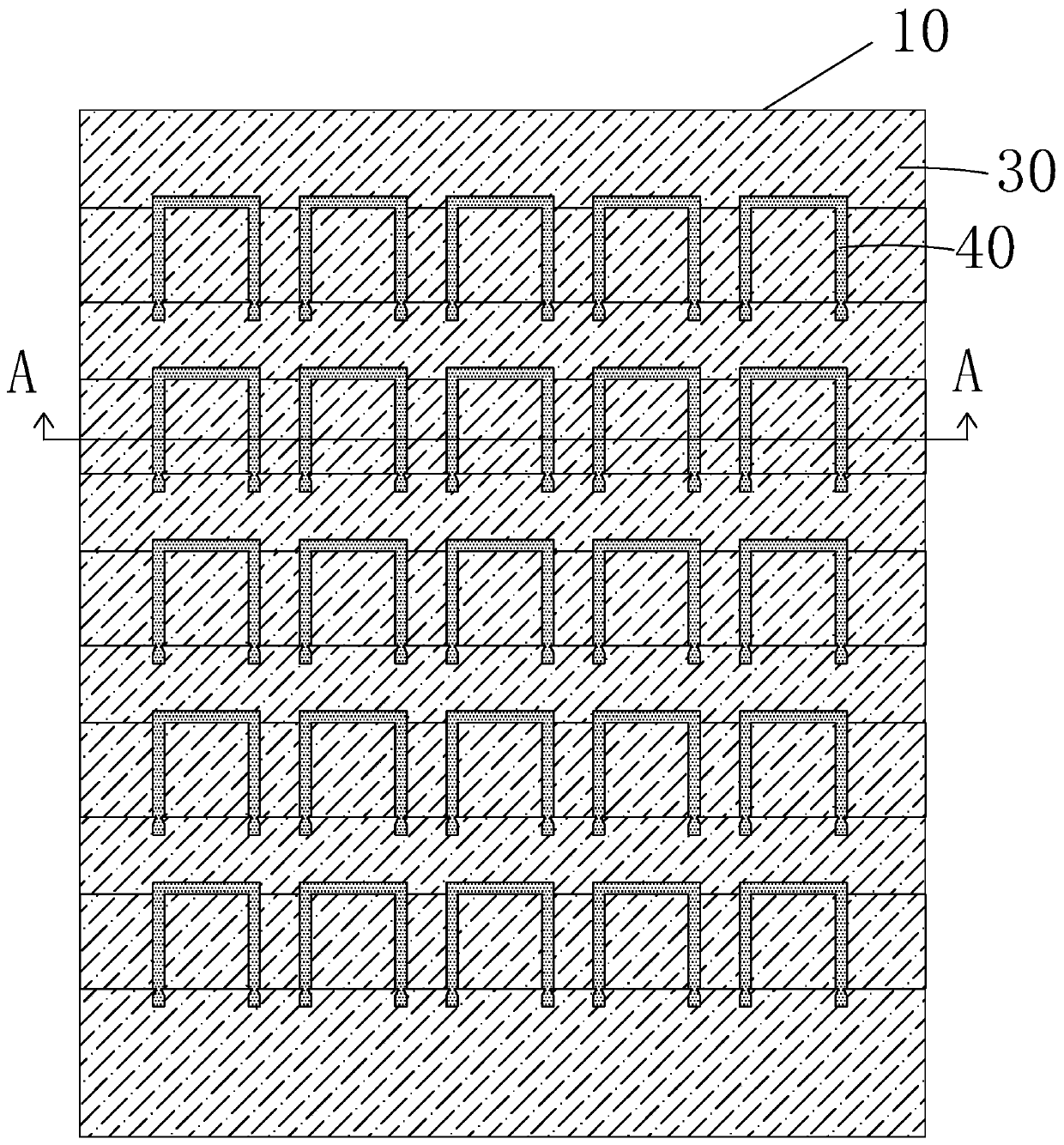
[0042] see Figure 14 , the present invention provides a method for manufacturing an LTPS array substrate, comprising the following steps:

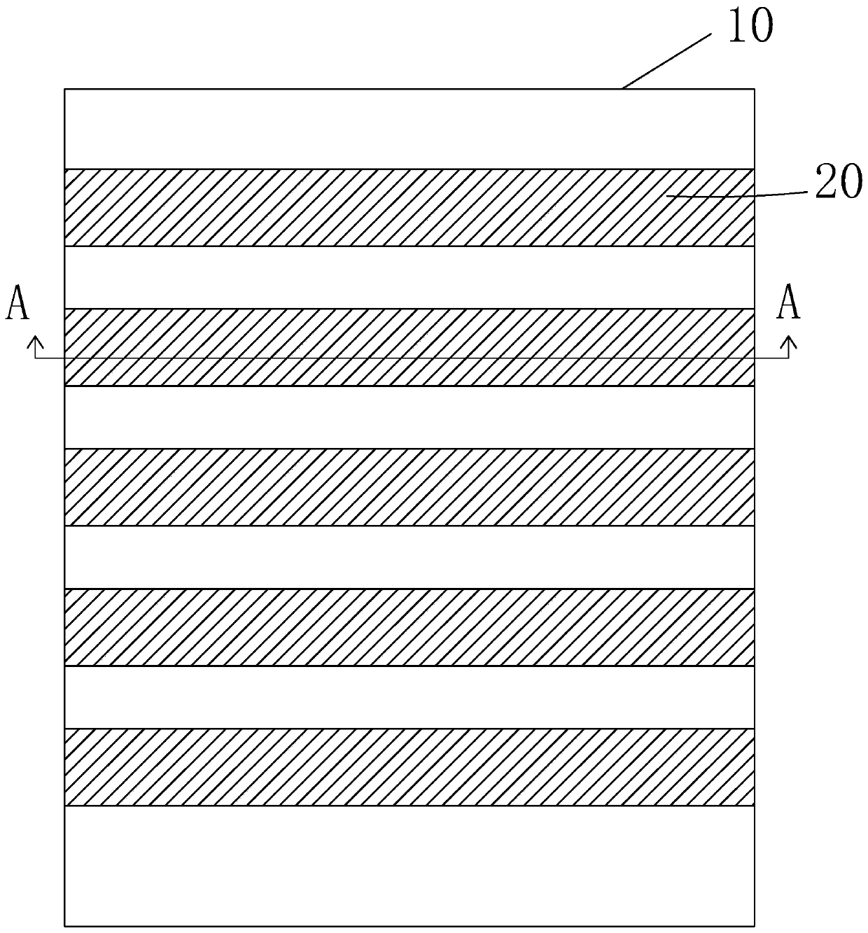
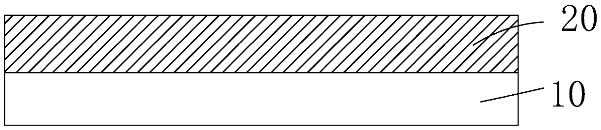
[0043] Step 1. Please refer to figure 1 and combine figure 2 , providing a substrate 10, depositing a light-shielding metal layer on the substrate 10, and patterning the light-shielding metal layer through a first photomask to obtain several light-shielding metal strips 20 arranged in parallel at intervals.

[0044] Specifically, in the step 1, the light-shielding metal layer is deposited by a physical vapor deposition method. The substrate 10 is a transparent substrate, preferably a glass substrate, and the material of the light-shielding metal layer is an opaque metal material, preferably molybdenum...


PUM


Abstract

The invention provides a production method of an LTPS array substrate. According to the method, one photomask is used for respectively patterning a light shielding metal layer and photoresist for performing N type heavy doping, thus forming a plurality of parallel spaced light shielding metal strips, and a plurality of photoresist strips overlapped one by one with the light shielding metal strips. By the production method, the number of photomasks required by production of the LTPS array substrate is reduced, the production cost is lowered, the displacement errors among membranous layers are reduced, the manufacture procedure precision is elevated, and the product quality is guaranteed.

Description

technical field [0001] The invention relates to the field of display technology, in particular to a method for manufacturing an LTPS array substrate. Background technique [0002] With the development of display technology, liquid crystal displays (Liquid Crystal Display, LCD) and other flat display devices are widely used in mobile phones, televisions, personal Various consumer electronic products such as digital assistants, digital cameras, notebook computers, and desktop computers have become the mainstream of display devices. [0003] Most of the liquid crystal display devices currently on the market are backlight liquid crystal displays, which include a liquid crystal display panel and a backlight module. The working principle of the liquid crystal display panel is to place liquid crystal molecules between two parallel glass substrates. There are many vertical and horizontal small wires between the two glass substrates. The direction of the liquid crystal molecules is ...

Claims


Application Information

Patent Timeline
Patent Type & Authority Patents(China)
IPC IPC(8): H01L27/12H01L21/77H01L21/027G03F7/20
CPCG03F7/20H01L21/027H01L21/77H01L27/1214H01L27/1259H01L2021/775
Inventor 张嘉伟
Owner WUHAN CHINA STAR OPTOELECTRONICS TECH CO LTD
Why Eureka
Try Eureka