Three-dimensional Dirac semimetal diffraction grating
A diffraction grating and semi-metal technology, applied in the optical field, can solve the problems of difficult generation and optimization of infrared pulse laser, high stability mode-locked pulse, poor stability, etc., and achieve easy high repetition rate ultrashort pulse and tunable working wavelength , High stability effect
- Summary
- Abstract
- Description
- Claims
- Application Information
AI Technical Summary
Problems solved by technology
Method used
Image
Examples
Embodiment 1
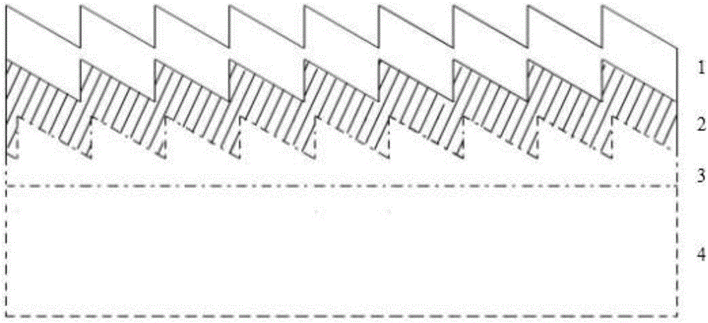
[0032] Embodiment 1: This embodiment provides a design scheme of a high-inversion three-dimensional Dirac semi-metallic diffraction grating 1 . combine figure 1 As shown, the specific scheme is as follows: reflective layer (3), including gold mirrors, silver mirrors and aluminum mirrors and high-reflectivity optical coatings, etc., is directly coated by methods such as magnetron sputtering, laser pulse deposition, electron beam evaporation, and thermal evaporation. Then use ultraviolet lithography, chemical etching, nanoimprinting and other methods to etch the strip-shaped periodic structure of the buffer layer material on the optical substrate (4), so that it has a diffraction function. On top of the reflective layer (3), magnetron sputtering, laser pulse deposition, electron beam evaporation, and thermal evaporation are used to prepare the buffer layer (2), and then the buffer layer is formed by ultraviolet lithography, chemical etching, and nanoimprinting. The material etc...
Embodiment 2
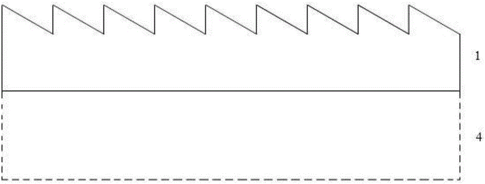
[0033] Embodiment 2: This embodiment provides a design scheme of a low-reflection three-dimensional Dirac semi-metallic diffraction grating. Specific designs, such as figure 2 As shown, the specific scheme is as follows: the Dirac semimetal in the functional layer (1) is directly coated on the optical substrate (4) by means of magnetron sputtering, laser pulse deposition, electron beam evaporation, and thermal evaporation, and then ultraviolet light is used to Engraving, chemical etching and nanoimprinting etc. will etch the Dirac semimetal strip-like periodic structure to make it have diffraction function. Finally, a passivation layer was coated on top of the Dirac semimetal using magnetron sputtering, laser pulse deposition, electron beam evaporation, and thermal evaporation.
Embodiment 3
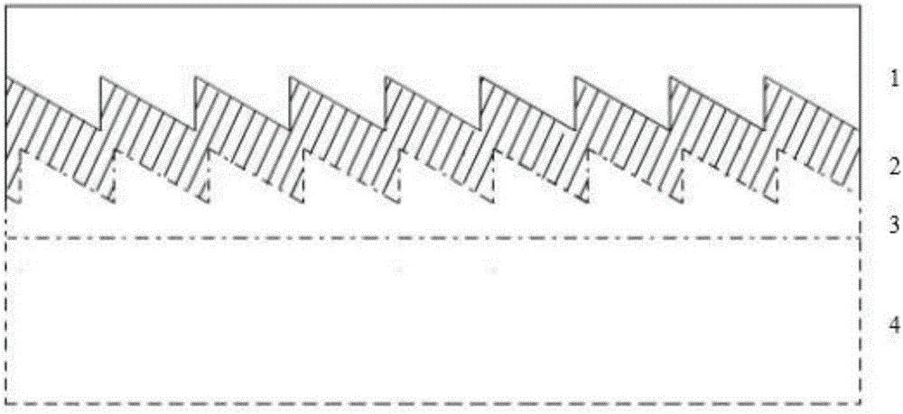
[0034] Embodiment 3: This embodiment provides a design scheme of a high-inversion three-dimensional Dirac semi-metallic diffraction grating 2 . Specific designs, such as image 3 As shown, first, the optical substrate (4) is etched with stripe-like periodic structures by methods such as ultraviolet lithography, chemical etching and nanoimprinting, so that it has a diffraction function. Secondly, reflective layer (3), including gold mirror, silver mirror and aluminum mirror and optical coating with high reflectivity, etc., is directly coated on the optical substrate ( 4), and use methods such as ultraviolet lithography, chemical etching and nanoimprinting to etch the reflective layer material into a stripe-shaped periodic structure, so that it has a diffraction function. Then, the buffer layer (2) is prepared on the reflective layer (3) by magnetron sputtering, laser pulse deposition, electron beam evaporation and thermal evaporation, etc. The stripe-like periodic structure i...
PUM
| Property | Measurement | Unit |
|---|---|---|
| Thickness | aaaaa | aaaaa |
| Thickness | aaaaa | aaaaa |
Abstract
Description
Claims
Application Information
 - R&D
- Intellectual Property
- Life Sciences
- Materials
- Tech Scout
- Unparalleled Data Quality
- Higher Quality Content
- 60% Fewer Hallucinations
Browse by: Latest US Patents, China's latest patents, Technical Efficacy Thesaurus, Application Domain, Technology Topic, Popular Technical Reports.
© 2025 PatSnap. All rights reserved.Legal|Privacy policy|Modern Slavery Act Transparency Statement|Sitemap|About US| Contact US: help@patsnap.com


