
Integrated type photoelectric storage device based on phase-change nano wires and testing method thereof

An integrated optical and testing method technology, applied in the field of nano-devices, to achieve high-density integration, good reliability, and low melting point

Active Publication Date: 2017-05-31
NINGBO UNIV
View PDF6 Cites 2 Cited by
  • Summary
  • Abstract
  • Description
  • Claims
  • Application Information

AI Technical Summary

Problems solved by technology

At present, there are no relevant research reports on memory devices that can simultaneously operate in the electrical and optical domains at home and abroad.

Method used


Image

  • Integrated type photoelectric storage device based on phase-change nano wires and testing method thereof
  • Integrated type photoelectric storage device based on phase-change nano wires and testing method thereof
  • Integrated type photoelectric storage device based on phase-change nano wires and testing method thereof

Examples


Embodiment 1

[0023] In Si 3 N 4 / SiO 2 / Si substrate is divided into two steps using electron beam-exposure and etching process to prepare devices, that is, first in Si 3 N 4 / SiO 2 / Si prepares electrodes and alignment marks, the electrodes are of Cr(10nm) / Au(90nm) structure with a total thickness of 100nm, and then the waveguide and vertical grating couplers are fabricated using electron beam-exposure and etching process again. The electrodes are distributed in Both sides of the waveguide. Finally, the GeTe nanowires were transferred to the Cr / Au electrode and hung vertically directly above the waveguide. The waveguide width of the device is 1.3 μm, the thickness is 200 nm, the distance between the electrode and the waveguide is 300 nm, and the short side and long side of the trapezoidal electrode are 4 and 20 μm, respectively. The grating period of the vertical coupler is 1.14-1.16μm, the fill factor is 0.88, and its coupling efficiency is about 27%. The length of the GeTe nanowire is a...

Embodiment 2

[0025] The difference is that the width of the waveguide suspended on the device is 1.4 μm, the thickness is 300 nm, the distance between the electrode and the waveguide is 500 nm, and the short side of the trapezoidal electrode is 5 μm. The length of the GeTe nanowire is about 3μm and the diameter is 300nm. The laser write pulse wavelength is 1.56μm, the power consumption is 5.2mW, and the detection light wavelength is 1.57μm.

Embodiment 3

[0027] The difference is that the distance between the electrode and the waveguide is 1 μm, and the short side of the trapezoidal electrode is 5 μm. The length of the GeTe nanowire is about 12 μm and the diameter is 400 nm. A focused ion beam (FIB) is used to plate Pt on the contact between the nanowire and the electrode to improve the ohmic contact between the nanowire and the electrode. At this time, the resistance of the device in the crystalline state is 1.2KΩ.

[0028] 2. Analysis of experimental results

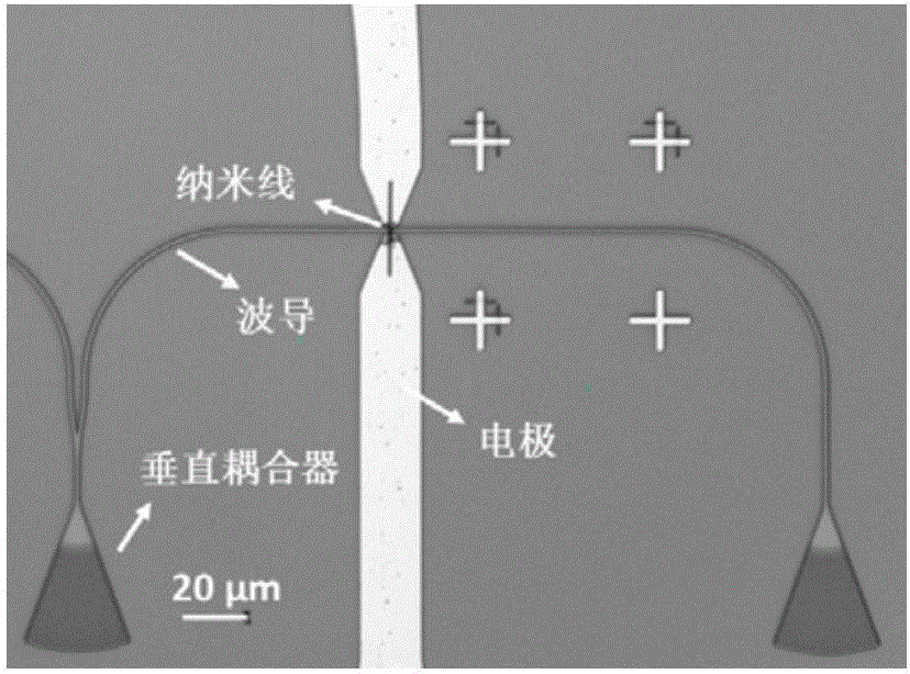
[0029] figure 1 This is an optical microscope image of the device of the present invention. The device is mainly composed of Si 3 N 4 Waveguide, Cr / Au electrodes on both sides of the waveguide, vertical grating couplers connected to both ends of the waveguide, and GeTe nanowires connecting the two electrodes. The diameter of the GeTe nanowire is about 700nm, the length is about 26μm, and its direction is perpendicular to the waveguide guided mode direction. The distance b...


PUM


Abstract

The invention discloses an integrated type photoelectric storage device based on phase-change nano wires and a testing method thereof. The integrated type photoelectric storage device is characterized by comprising a waveguide, wherein the two ends of the waveguide are respectively connected with a grating vertical coupler; electrodes are symmetrically distributed at the two sides of the waveguide; the phase-change nano wires are arranged above the waveguide and are vertical to the waveguide; and the phase-change nano wires are connected with the two electrodes to form ohmic contact. The integrated type photoelectric storage device and the testing method disclosed by the invention have the advantages that the simultaneous operation in an electric domain and a frequency domain can be realized, multi-stage storage can be realized by utilizing a photoelectric hybrid mode, the transient process of the phase-change nano wires can be monitored and the phase-change speed can be tested.

Description

Technical field [0001] The invention relates to the field of nano devices used for photoelectric hybrid storage, in particular to an integrated photoelectric storage device based on phase change nanowires and a testing method thereof. Background technique [0002] Nano-photonic integrated components combined with electronic integrated devices can construct on-chip multifunctional optoelectronic circuits to achieve efficient data storage, communication and processing in a single on-chip system. This kind of multi-functional on-chip integrated optoelectronic device with smaller size and power consumption allows simultaneous operation in the electrical and optical domains, and can process opto-electric hybrid mode data, facilitate the management of large amounts of information and reduce the complexity of multi-function integration . The performance of this type of optoelectronic hybrid device mainly depends on the multifunctional material that has both electrical and optical rapid...

Claims


Application Information

Patent Timeline
Patent Type & Authority Applications(China)
IPC IPC(8): G11C11/42
Inventor 吕业刚张巍沈祥王国祥徐培鹏
Owner NINGBO UNIV
Learn More