
High-mobility transistor and preparation method thereof

A high-mobility, transistor-based technology, applied in semiconductor/solid-state device manufacturing, semiconductor devices, electrical components, etc., can solve the problems of lack of inverters, etc., and achieve the effect of good manufacturing process compatibility and simple device structure

Inactive Publication Date: 2017-05-31
PEKING UNIV
View PDF4 Cites 4 Cited by
  • Summary
  • Abstract
  • Description
  • Claims
  • Application Information

AI Technical Summary

Problems solved by technology

However, in the field of digital circuits, there is still a lack of mature inverters built with complementary devices similar to CMOS.

Method used


Image

  • High-mobility transistor and preparation method thereof
  • High-mobility transistor and preparation method thereof
  • High-mobility transistor and preparation method thereof

Examples


Embodiment 1

[0030] Implementation example 1: GaN-based HEMT with P-type graphene channel

[0031] (1) Preparation of GaN epitaxial layer

[0032] The MOCVD method uses organic compounds of group III elements and hydrides of group V elements as raw materials, and is brought into the reaction chamber by a carrier gas such as hydrogen or nitrogen to epitaxially form compound single crystal thin films on a substrate heated at high temperature. The growth of GaN material is the epitaxial growth of GaN thin layer realized by the chemical reaction of Ga decomposed by TMGa and the cracked N atoms of NH3 at high temperature. The growth of GaN requires precise control of the growth temperature and the flow rate and partial pressure of NH3, and the flow rate of TMGa and other parameters. The commonly used methods are conventional MOCVD (including APMOCVD, LPMOCVD), plasma enhanced MOCVD (PE-MOCVD) and electron cyclotron resonance assisted MBE. Sapphire substrate cleaning: (H 2 SO 4 :H 3 Etch in...

Embodiment 2

[0042] Implementation example 2: GaN-based HEMT with N-type graphene channel

[0043] (1) Preparation of GaN epitaxial layer

[0044] The MOCVD method uses organic compounds of group III elements and hydrides of group V elements as raw materials, and is brought into the reaction chamber by a carrier gas such as hydrogen or nitrogen to epitaxially form compound single crystal thin films on a substrate heated at high temperature. The growth of GaN material is the epitaxial growth of GaN thin layer realized by the chemical reaction of Ga decomposed by TMGa and the cracked N atoms of NH3 at high temperature. The growth of GaN requires precise control of the growth temperature and the flow rate and partial pressure of NH3, and the flow rate of TMGa and other parameters. The commonly used methods are conventional MOCVD (including APMOCVD, LPMOCVD), plasma enhanced MOCVD (PE-MOCVD) and electron cyclotron resonance assisted MBE. Sapphire substrate cleaning: (H 2 SO 4 :H 3 Etch in...

Embodiment 3

[0054] Implementation example three: AlN-based P-type-graphene channel HEMT

[0055] (1) Preparation of AlN epitaxial layer

[0056] The MOCVD method uses organic compounds of group III elements and hydrides of group V elements as raw materials, and is brought into the reaction chamber by a carrier gas such as hydrogen or nitrogen to epitaxially form compound single crystal thin films on a substrate heated at high temperature. The growth of GaN material is the epitaxial growth of GaN thin layer realized by the chemical reaction of Ga decomposed by TMGa and the cracked N atoms of NH3 at high temperature. The growth of GaN requires precise control of the growth temperature and the flow rate and partial pressure of NH3, and the flow rate of TMGa and other parameters. The commonly used methods are conventional MOCVD (including APMOCVD, LPMOCVD), plasma enhanced MOCVD (PE-MOCVD) and electron cyclotron resonance assisted MBE. Sapphire substrate cleaning: (H 2 SO 4 :H 3Etch in P...


PUM


Abstract

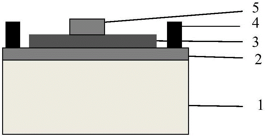
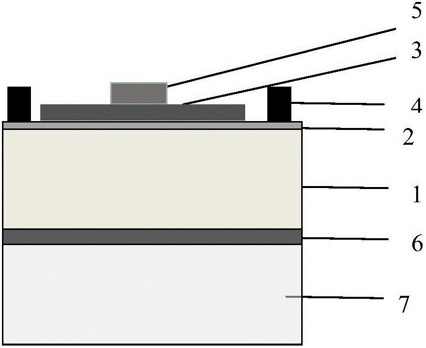
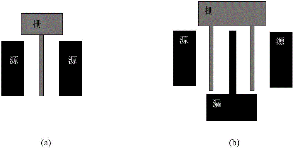
The invention discloses a high-mobility transistor and a preparation method thereof, and belongs to the field of a functional electronic device. A high-mobility double-layer or three-layer graphene film is utilized as an electronic transport channel, and conductivity property thereof is modulated by stress and doping characteristics; when voltage is added to a gate end, the current in the channel is adjusted, thereby realizing function of an HEMT device; since the double-layer or three-layer graphene film conductivity chances with doping, an N-type HEMT and a P-type HEMT can be prepared on the same GaN simultaneously; and the N-type HEMT and the P-type HEMT form a phase inverter of a digital logic circuit, thereby realizing radio frequency and microwave frequency band digital logical operation function.

Description

technical field [0001] The invention belongs to the field of functional electronic devices, in particular to a double-layer graphene structure with high electron mobility as an electron transport channel and a high mobility transistor (HEMT) derived from the structure. Background technique [0002] A high electron mobility transistor (HEMT) is a field effect transistor that uses a two-dimensional electron gas with high mobility to work. This device and its integrated circuit can be well applied to ultra-high frequency (millimeter wave), ultra- high-speed field. In a conventional HEMT device, due to the large discontinuity difference in the conduction band of the heterojunction contact, a triangular quantum well is formed on the side of the narrow bandgap semiconductor at the interface, and a potential barrier is formed on the side of the wide bandgap semiconductor to limit the triangular quantum well. The free electrons in the well move in the direction vertical to the cont...

Claims


Application Information

Patent Timeline
IPC IPC(8): H01L29/778H01L29/423H01L21/335
CPCH01L29/423H01L29/66431H01L29/778
Inventor 周劲傅云义
Owner PEKING UNIV
Learn More